When I have said "esoteric" I mean, not lot of us have-them in stock on their bench. Is your version definitive, so I can test-it intensively, or did I understood you were sayin some refinements to come ? Too, please, could-you provide us technical argues for your preferences between your version (if definitive) and my last one (largely inspired by you ;-) ? Thank in advance.I chose devices that can be either-or. My preference is for surface mount using the Diodes Inc devices..
LTSPice has some strange behaviors. Looking at the offset at various temperature, I was unhappy with the offset variations seen in AC simulations. Attached, the result of .trans with the servo on at 50°. Generator set to 0V, both windows looking, in the same time to the same output of the same simulation. Ouf ! The servo is working damn well and we don't have to worry.
And, as, in this situation, the servo output is at some 667mV, and the opamp allows some +/- 11V, we still have A LOT of margin.
I was probably very tired the first time I tested, or I tried with other devices. The spladski version as it validate perfectly too the tempco: -10° 130mA 0 ° 109.7mA 50° 51mA 70° 44mA 75° 43mA No problem neither with the VAS from 13mA to 5.6mAit had seem to me your version was increasing the power device current with the increase of temperature ?
Very good phase (64°) and gain (19dB) margin. Congratulations. It smells good.
Tomorrow, I will test how it behaves with input devices mismaches and distortions.
Attachments

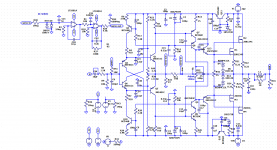
Quite fascinating to see the schematics in post #1 (attached to the right) shares so many components, drawn in the same way and even have the same component location numbering as the attached schematics to the left, professor, does your inspiration have its roots in Mr Christophe Esperado's CFA Crescendo amplifier? 😎🙂
BTW, he is a member here on DiyA, but unfortunately banned, perhaps your former life/alter ego? 😀
www.esperado.fr - Le crescendo revisité
BTW, he is a member here on DiyA, but unfortunately banned, perhaps your former life/alter ego? 😀
www.esperado.fr - Le crescendo revisité
Attachments
Last edited:

No surprise. I simulated, two years ago, this crescendo, and, when I had this idea to explore a CFA with high loop gain the cascode was a requisite, so I started from its asc file to get rid of the VAS/ power stage re-design, saving time. It is a very classical implementation.perhaps your former life/alter ego? 😀
But, again, the subject is the amp, not my person: I'm the real Professor Tournesol.
Usually, CFAs have low loop gain, and extended bandwidth while VFAs are the contrary. My question was to see what will happen if we try to mix the two, in order to figure out if the difference in listening impression between CFAs and VFAs depends on the slew rate/ extended low loop gain or just the current on demand.
BTW, We have lost an idea in the process of refining this design, that was to use the +- 12 V to set the offset compensation bridge and get rid of some AC parasitic, as the +- 12V will, of course, be regulated.
Last edited:
Yes, it is about the circuit, and now I better understand the changes made to a perfectly good and sensible amplifier to end up with a lot of issues. It looked to me as if two people designed two parts of an amp and then glued them together. That was what puzzled me before, and what I understand now.
Jan
Jan
Funny remark (quite aggressive and very unfair for the work done by the contributors), as It is the exact opposite that happened.Yes, it is about the circuit, and now I better understand the changes made to a perfectly good and sensible amplifier to end up with a lot of issues. It looked to me as if two people designed two parts of an amp and then glued them together. That was what puzzled me before, and what I understand now.
We started with a rough and minimal scheme supposed to work, but that had some potential issues IRL. With the help of Spladski, we end-up with NO ISSUE at all and two solutions to get rid of the native problem of diamonds. And, looking at the original schematic, with very little changes.
The first solution (the one with variable resistances) is precise, but request tuning of those on the bench, the one of spladski is less precise, but get rid of this tuning.
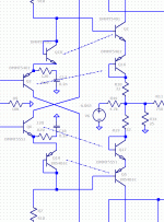
One little explanation about this. As we use a diamond like topology to get rid of the VBE voltage difference between input and feedback (and the electrolytic big cap that usually comes with) but with max gain, all VBE mismatches are amplified by the gain. And, as the current in the second stage is set by the emitter voltage of the first one, it will vary with the VBEs of both. In other words, the current of the first input stage is set by the current sources, but any missmatches between this stage and the second will impact the current in the second one and the VAS. We need some margin because, if the VBE of the transistors second stage is higher than the one of the first transistors, the second one will not conduct. And, if it is the contrary, the second will over conduct.
The add of a diode in the second stage ensure that the VBE+diode will always be higher than the first stage. IE, that it will never over conduct. And the adj1 & adj2 resistance to add the necessary voltage in his base to make the second transistor +diode conducting as we want whatever it happens.
The clever idea of spladski is to use a matched pair, supposed to have similar VBEs to reduce the mismatches. The second transistor, replacing the diode in serial with the second transistor emitter reduce the differences, as the two VBEs are now in serial in the second stage. IE any VBE variation in the first stage is reflected by the second transistor of the pair in the second stage The inconvenience is the variation of the second stage current, while reduced, still exists. Hence its change of the cascode to allow-it to accept this variation.
My solution is to simply tune the VBE differences with adjustable resistance to set the second stage current to 1.2mV whatever it happens.
VBE problem is solved, NO temperature issue. As I said, problems solved and "we end-up" with NO ISSUES. At all, because both phase and gain margins are good enough to make a very stable amplifier.
This gave-me an idea, expanding the spladski one. In the original schematic, the inconvenience we the need of closely matching the VBEs of the first and second stage NPN/PNP or PNP/NPN transistors. Working, but not user friendly. Supposing that the DMMT5401 pairs are closely matched on VBEs between their two transistors, why not using those pairs to compensate each others both sides ?The clever idea of spladski is to use a matched pair, supposed to have similar VBEs to reduce the mismatches. The second transistor, replacing the diode in serial with the second transistor emitter reduce the differences, as the two VBEs are now in serial in the second stage. IE any VBE variation in the first stage is reflected by the second transistor of the pair in the second stage The inconvenience is the variation of the second stage current, while reduced, still exists.
Attached a modified spladski schematic, not tested, just to explain. If VBE Q18 = VBE Q1 =X (one pair), and VBE Q2 = VBE Q16 = Y (second pair), we get VBE first stage = Y+X and VBE second stage = X+Y. And, as the current in first stage is fixed by the current sources, the second will be the same whatever X and Y mismatches. The best of the two worlds: Precise result and no tuning requested.
Comments ?
Attachments
Haha! Two post from you and one contradicts the other! I couldn't make this up!
Edit: no aggressiveness intended at all! But you must understand that for an experienced designer, it is clear that that circuit comes from different people. And that these people differ in experience and expertise. It is what it is.
Jan
Edit: no aggressiveness intended at all! But you must understand that for an experienced designer, it is clear that that circuit comes from different people. And that these people differ in experience and expertise. It is what it is.
Jan
Last edited:
Please, could-you find an other playground where you can flourish your negativity and personal attacks at leisure ? How many simulations have you done on this project, and where are your brilliant proposals, your schematics and their simulated results ?Haha! Two post from you and one contradicts the other! I couldn't make this up!
What I read under your pen are free and personal critics, never supported by any convincing data. And ad hominem.
As you said, we don't need your help. Especially of this kind, mister self proclaimed "Experienced designer" that seems to misunderstand everything from the beginning.
"No aggressiveness intended ", but that is enough OOT.

Last edited:
I tried earlier, not to give specifics like 'change this R to that, connect this to that instead' because I know there will be resistance (no pun intended) to that. Instead I tried mentioning the concepts how to solve the Vbe and tempco mess, hoping the idea would come across. That didn't stick either.
And why would I sim this circuit? Surely you can also read a circuit and know where the obvious problems lie??
And please, do not see everything that is not immediate praise as a personal attack. You really have to lighten up! It's audio, not a matter of life and death!
Jan
And why would I sim this circuit? Surely you can also read a circuit and know where the obvious problems lie??
And please, do not see everything that is not immediate praise as a personal attack. You really have to lighten up! It's audio, not a matter of life and death!
Jan
May-be your capacitance to understand the way I'm functioning, which, I agree, is kinda special ? ;-)I tried earlier, not to give specifics like 'change this R to that, connect this to that instead' because I know there will be resistance (no pun intended) to that.
Sorry, but I have not seen any "concept how to solve" from you till now. Only reports of problems we already knew.Instead I tried mentioning the concepts how to solve the Vbe and tempco mess, hoping the idea would come across. That didn't stick either.
The tempco question is well known as well as various solutions. It is usually the last thing to take care of.
It is like the little part of a schematic i just posted. No need to tell-me that, with the emitters degenerative resistances in the second stage, it will never work. As it was not the purpose, I neglected to remove them. It was just to show the arrangement of the transistors.
On the other hand, considering your great experience, and the fact that I have not often used such beasts, I would be interested to know the average tolerance of the VBEs in a "matched pair".
Last edited:
from looking at the data sheets, they spec Vbe in different grades, 1mV, 2mV etc, usually the 1,2mV grade they spec a 10% hfe match. The old one I looked at was a TI part 2n2920? it is still in production, but is expensive.I would be interested to know the average tolerance of the VBEs in a "matched pair".
Buy your bjts on paper tape, they seem to have tight matching from what I have been measuring with the current supply. With bulk I would think there is more variation in singles.
On the other hand, considering your great experience, and the fact that I have not often used such beasts, I would be interested to know the average tolerance of the VBEs in a "matched pair".
The idea I tried to bring across was to make it such that the Vbe match would no longer be an issue.
Vbe matching or Hfe matching often is unavoidable in open-loop situations, but not here.
What I would ask is: the original amp was complete and working well. What is your aim to change or improve in terms of performance? That should drive the development.
I will never forget Bruno Putzeys motto: The road to hell: specify the design and accept the performance; The road to heaven: specify the performance, accept the design.
Jan
Last edited:
Many thanks, Rsavas.from looking at the data sheets, they spec Vbe in different grades, 1mV, 2mV etc, usually the 1,2mV grade they spec a 10% hfe match. The old one I looked at was a TI part 2n2920? it is still in production, but is expensive.
Buy your bjts on paper tape, they seem to have tight matching from what I have been measuring with the current supply. With bulk I would think there is more variation in singles.
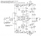
In the two versions of the schematic, please indicate by q number the needed thermal coupled devices
In the V7, (post 230In the two versions of the schematic, please indicate by q number the needed thermal coupled devices
Pizzicato, a 200W low distortion CFA amplifier)
as we need a cooler, may-be we could align on a plate Q9, Q13, Q10, Q14 ?
For the input stage, I have no idea if this is needed as we use a servo, they all are very close (and low) on current.
For the spladski version (definitive ?) I prefer to let him decide for its input. For VAS and driver, it will be the same in the two versions.
I tried this idea of crossed matched devices. It works fantastic on currents, with +-2mV of VBE mismatch. It add a lot of stability margin, and allow much faster SR. Should be a definitive solution.
BUT, for some reason, distortion increase a lot. In a way that let-me think LTSPICE turn crazy. Is-it a question of models ? I'm very uncomfortable with simulations. And I have no time to simulate the Spladski version for distortion before one or two days.
Adding that Dadod had let a bomb "I tried to simulate your amp, but get very strange result" without more details and give no more news, may-be it should be careful to wait a little more before to start the input stage final board design ?
In the V7, (post 230
Pizzicato, a 200W low distortion CFA amplifier)
Please, note that R45 is 11ohms, I assume it needs to be 110.
Kind regards
Oh, I provided the wrong link, this is the Spadski version. The V7 is in #238.Please, note that R45 is 11ohms, I assume it needs to be 110.
Kind regards
Anyway, this resistance value don't change the behavior a lot, but thanks for the tip ;-)
Last edited:
Tournesol;5 Adding that Dadod had let a bomb "[I said:I tried to simulate your amp, but get very strange result[/I]" without more details and give no more news, may-be it should be careful to wait a little more before to start the input stage final board design ?
To much changes in this for my taste, I'll wait until you get close to final schematic.
Just LG plot I've got and think PM and GM should be increased, bandwidth too.
Attachments
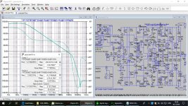
daodad, I'm uncertain how to interpret your AC analysis plot. Does it indicate that the amplifier's open loop gain bandwidth product is (5.27E6 * ClosedLoopGain)? And therefore the closed loop bandwidth is 5.3 MHz? That's quite a bit higher than the closed loop bandwidths in, for example, Bob Cordell's book. Those mostly have OLGBWP of approx 10 MHz and a closed loop bandwidth of approx 0.5 MHz.
_
_
Last edited:
- Home
- Amplifiers
- Solid State
- Pizzicato, a 200W low distortion CFA amplifier