I just wanted to make people aware that the servo output is identical to the amp DC offset only amplified (and inverted, normally, unless you use a non-inverting servo). So adjusting the DC offset by adjusting for zero servo output is much more precise than looking at the actual amp output.
Jan
Jan
Of course, once stabilized, the sims with this servo show an offset in the Picovolts range at the amp output. And, as the servo voltage is applied to the - input, in the same sens that the one of it.
Yes, until the day that we have opamps with infinite gain, there is always a residual offset, otherwise the servo cannot work. The servo needs *some* input to give an output so you always need *some* output offset.
As you have noted, the output offset can be very, very small, and is thus hard to null even with a good multimeter. And you really want to adjust the offset to get the servo in the middle of its operating range, to have the largest 'tracking' range for DC drift. Hence the suggestion to look at the servo output; if that is zero, amp DC output is also zero.
I like to drill down into the details of what is going on for better understanding, but in reality it isn't very important as even 10mV of DC offset at the amp output is totally irrelevant.
What I should add is that you can't very well see a difference in amp DC offset with the servo output at zero or with the servo output close to one of the opamp supply rails. In both cases the DC offset looks very small, but in the latter case, the servo tracking range to correct for drift is very small close to its supply.
So it is important to adjust the offset and make sure the servo is in the middle of its range, which normally is zero. This should also be verifiable in LTspice.
Jan
It seems it is more than hard: impossible in this forum ?It's hard to manage a design by committee but you seem to have it in hand.
I proposed a gross scheme of a promising CFA amplifier "in progress" to be a collaborative work, to see how, together, with the add of all our expertise, we could achieve something interesting at the end.
Only two members were really interested to collaborate. The others seeming to take pleasure in pointing out the defects of the initial project, a defect of which, of course, we were obviously aware.
Krisfr who propose to design the board, and Spladski with a lot of nice ideas to address all the flaws of the original scheme that needed to be fixed.
Mot of thanks to them, and all the other's comments.
I had spend a lot of time, simulating dozens of sim files, trying to get the best of all. But, suddenly, when i tried to establish a working version (V7), renumbered for we could talk together, communication had seem to be suddenly totally broken.
It seems obvious that we have to keep a minimal discipline and friendly exchanges (the only pleasure of this purpose) if we want to progress.
Was I too brutal in my way of refocusing the debate? Probably, but it was, of course not in my intention to be unpleasant in any way. If this is the case, accept my apologizes.
Pushing further the brilliant idea of spladski to use matched dual devices (2mV VBE matched), in a symmetric configuration between the first and the second stage of the input stage, all my sims demonstrated it was the solution to address all the flaws. At this point all communication had seem to be broken.
Also, in a sorrow way, I do not know if it is worthwhile to continue the work undertaken, despite the fact that my V8 version, fruit of all this work, actually under lot of simulation that will take some times, summary of all the best suggestions, seems to answer all the criteria of a successful project.
It would certainly be all the more a pity if working together, explaining each detail allows many visitors to learn things.
So time to ask a question, Krisfr and Spladski, are-you still interested we continue together up to the end ?
Last edited:
Thanks a lot Krisfr. Waiting to read you 🙂 I am near ready to give-you a full schematic.In a word, Yes. But I will have more to say later today.
Question to all: What are the pro and cons between Zeners and LED, as current sources references (Noise, precision, temp behavior) ?
Pizzicato V8.
The end ?
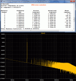
HD 1000 Hz, without error correction: 0.000072%
HD 1000 Hz, with error correction: 0.000008%
Tempco (quiescent current mosfets):
10°: 160mA
27°: 145mA
50°: 126mA
Bandwidth: 2 Hz-4,5MHz (-3dB)
Phase margin: 72°, gain margin: 14dB.
Thanks to Spladski, and its idea to use matched transistor pairs both as transistors and diode, because they are matched at <2mV VBE, thermally coupled in the same chip, and with my idea to balance the two stages with them, we have succeeded to get rid of all the possible problems that many members had underlined.
The same PNP and NPN pair is now used half in the first stage of the input stage, and the other half in the second stage, both NPN and PNP in each half stage, the two stages are now totally locked together, with the same current provided by a current source. No more tuning or adjustments requested apart quiescent current, offset voltage and error correction max rejection.
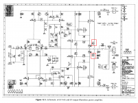
Theory of operation.
The input signal is filtered by R1 & C2 to ensure that it will never exceed the slew rate of the amp and to remove unwanted HF parasitics, before to enter in the QP1-1 & QP2-1 transistors working as emitter followers. At their output, it crosses one transistor QP3-1 & QP4-1 mounted as a simple diode (base-emitter). The DC of the signal is, now, the sum of the VBE of QP1-1+QP3-1 & QP2-2+QP4-1.
The current of this stage is fixed by the current sources constituted by Q3-Q4. The base voltage reference is fixed by a Zener Z1 & Z2 in serial to one diode (D3 & D4) for temperature compensation.
This stage is out of the feedback loop.
The second stage of the input stage use the same pair transistors to compensate in reverse order the initial VBE. AS they are matched with the first stage and thermally coupled, the compensate exactly this VBE: VBE (QP1-1+QP3-1) = VBE (QP1-2+QP3-2). And same thing for the symmetrical bottom part.
The collectors of QP1-2 &QP2-2 will be at ground DC: No need for a cap in the feedback path.
Now, as the feedback is applied at the emitter of the second stage transistor, this one is not used as an emitter follower, like a pure diamond, but amplify the input signal: their collector output use the resistance R15 & R16 to achieve this. The current across them (the same as the one o of the current sources fixes a voltage applied to the base of the Cascoded VAS : the current of the cascode is fixed by this voltage. Hence, the use of two diodes DA5 & DA7 to fix-it around 10mA. They are part of the thermal compensation as well. The gain of the VAS is fixed by R27 & R28 resistor.
All what follow is classical: A transistor used to fix the quiescent current in the power devices, witch is part of the thermal compensation, a classical driver (his current is fixed by R29) and the power devices.
The Lateral power FETs do have a mismatch of their gate parasitic capacitance (900pf VS 600pF). The CP1-> CP7 are here to approach them.
The resistances R31 toR 38 are gates stoppers. On the schematic, they are 56 Ohms, it can be increased to 110 or 220 Ohms with no major changes.
The quiescent current of the power FETs is fixed around 150mA. That the approximate point where they are thermally neutral, after what they have a thermally negative curve: this tend to stabilize this quiescent a little more and gives a good margin in class the class A operation of this Class AB amplifier.
The end ?
HD 1000 Hz, without error correction: 0.000072%
HD 1000 Hz, with error correction: 0.000008%
Tempco (quiescent current mosfets):
10°: 160mA
27°: 145mA
50°: 126mA
Bandwidth: 2 Hz-4,5MHz (-3dB)
Phase margin: 72°, gain margin: 14dB.
Thanks to Spladski, and its idea to use matched transistor pairs both as transistors and diode, because they are matched at <2mV VBE, thermally coupled in the same chip, and with my idea to balance the two stages with them, we have succeeded to get rid of all the possible problems that many members had underlined.
The same PNP and NPN pair is now used half in the first stage of the input stage, and the other half in the second stage, both NPN and PNP in each half stage, the two stages are now totally locked together, with the same current provided by a current source. No more tuning or adjustments requested apart quiescent current, offset voltage and error correction max rejection.
Theory of operation.
The input signal is filtered by R1 & C2 to ensure that it will never exceed the slew rate of the amp and to remove unwanted HF parasitics, before to enter in the QP1-1 & QP2-1 transistors working as emitter followers. At their output, it crosses one transistor QP3-1 & QP4-1 mounted as a simple diode (base-emitter). The DC of the signal is, now, the sum of the VBE of QP1-1+QP3-1 & QP2-2+QP4-1.
The current of this stage is fixed by the current sources constituted by Q3-Q4. The base voltage reference is fixed by a Zener Z1 & Z2 in serial to one diode (D3 & D4) for temperature compensation.
This stage is out of the feedback loop.
The second stage of the input stage use the same pair transistors to compensate in reverse order the initial VBE. AS they are matched with the first stage and thermally coupled, the compensate exactly this VBE: VBE (QP1-1+QP3-1) = VBE (QP1-2+QP3-2). And same thing for the symmetrical bottom part.
The collectors of QP1-2 &QP2-2 will be at ground DC: No need for a cap in the feedback path.
Now, as the feedback is applied at the emitter of the second stage transistor, this one is not used as an emitter follower, like a pure diamond, but amplify the input signal: their collector output use the resistance R15 & R16 to achieve this. The current across them (the same as the one o of the current sources fixes a voltage applied to the base of the Cascoded VAS : the current of the cascode is fixed by this voltage. Hence, the use of two diodes DA5 & DA7 to fix-it around 10mA. They are part of the thermal compensation as well. The gain of the VAS is fixed by R27 & R28 resistor.
All what follow is classical: A transistor used to fix the quiescent current in the power devices, witch is part of the thermal compensation, a classical driver (his current is fixed by R29) and the power devices.
The Lateral power FETs do have a mismatch of their gate parasitic capacitance (900pf VS 600pF). The CP1-> CP7 are here to approach them.
The resistances R31 toR 38 are gates stoppers. On the schematic, they are 56 Ohms, it can be increased to 110 or 220 Ohms with no major changes.
The quiescent current of the power FETs is fixed around 150mA. That the approximate point where they are thermally neutral, after what they have a thermally negative curve: this tend to stabilize this quiescent a little more and gives a good margin in class the class A operation of this Class AB amplifier.
Attachments


Theory of operation: Error correction and servo.
The principle is to subtract the original signal from the output signal of the amplifier. This is done by the U101 where R102 is used to adjust their levels in order to get the best levels /match before this subtraction. This is done first minimizing the output signal, then trying to get the original frequency at 90° of phase.
In an perfect world, the output of this subtraction contain only the distortion and the offset error.
This little remaining signal (~3mV) is amplified by U103 before to be applied to the negative input of the CFA power amplifier. This add 10dB of gain to the feedback, without adding loop gain.
The same "error only" signal is integrated in U102 by the C103 capacitance that reject all remaining frequencies of the audio signal and only out the DC error that is applied again in the - input of the power amp.
That's a new kind of servo. With the obvious advantage that the musical signal being near suppressed, both by the subtraction and the integrator, no sonic character of the Op Amps will be heard, and that the margin of the servo is increased: faster and more powerful. The resulting offset is in the nano-volts.
That's all, folks, apologize for my poor English.
Last edited:
Indicate test points and jumpers Big diode on output, MURS3230 type Wattage of all transistors and resistors Indicate the type of capacitor, i.e. polyester or otherwise Op amps on ips or not, think so but want to be sure.
Draw a line to designate what goes on small board Source of + - 12 volts and topology I wanted to create a more or less output board that could accommodate a standardized ips board to be able to do comparisons of different approaches to design typologies.
I would like to have at least a few words of input on the use of the Greenamp power technology that was developed by Ostripper. I do not ever want to use that or any technology without consent of the creator of said technology. Ethics here are of importance. I have some questions about the use of PCBway 100 sq boards and I will have to solve them before I proceed any further with actually ordering them. But that will not stop my development of the needed board for this project. So much for the I's😀
Please let me know which of the 2 or 3 boards should come first and so on. This is my direction and will try to do a good job on these. Please let me know of any improvements and or suggestions as I will post as I go along. DIYaudio has taught me a lot, and I hope to learn more about LTSpice and the use of the TIAN probe and measuring THD. I need a mentor. I am a digital CPU kinda guy for too many years. But I think if I can learn these as well as I know AutoCad and a Tektronics 2465 I will be okay. An easy plugable IPS on a stable Output of 4 to 8 OUTput devices is the key to finding which design SOUNDS the best and not which one has the greatest specs.😛 Thanks
Krisfr, If you have LTSpice, most of your questions will be answered in it about components, with a right click on them from the .as file. I will be there to answer your questions.Indicate test points and jumpers Big diode on output, MURS3230 type Wattage of all transistors and resistors Indicate the type of capacitor, i.e. polyester or otherwise Op amps on ips or not, think so but want to be sure.
Draw a line to designate what goes on small board Source of + - 12 volts and topology I wanted to create a more or less output board that could accommodate a standardized ips board to be able to do comparisons of different approaches to design typologies.
Jumpers and test points will be indicated as well.
Middlebrook is implanted on the AS file. Don't hesitate to ask me by PM if you need more precision on how to use-it as well as Tian.
I do not understand "Big diode on output and MURS3230" as they don't exist on the schematic. Please, could-you explain ?
Nothing special about +&- 12V. The same regulated PSU will be used for the OP amps. I think it should be better to have them on a separate board. This board could contain the logic for the protection... or not...as you feel.
I don't think it is possible to use the input stage on other VAS, not specially designed for-it, as the voltage at R15/R16 fix the VAS current Even a small change of their values can drive-it out of limits. Only the Output stage is classical... as long as they use MOSFETS. On my opinion, it is a bad idea to build this amp in several boards. Better to try to optimize the all amp circuit.
We can discuss all this more deeply and look at the pro and cons.
Thanks, Krisfr. I'm so happy to have-you here.on this project.
Help and advices
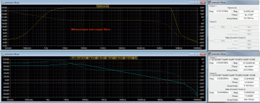
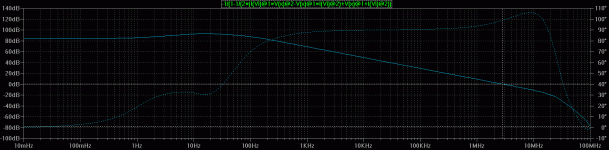
Working on compensations, I had this beautiful result with Midlebrook method. (See attached) BUT, when I run the trans, it takes hours like if something was not correct (oscillations?) I have my CPU hot before the end, don't know how it will end. I need help from the LTSPICE experts.
Can't we lie on the Midlebrook sims, or sir Niquist was wrong and I have to prepare a paper for the academy before to fire my moon rocket? Or is-it just that LTSPICE has too much work on phases at trans. simulation and it will end nicely, as expected?
Thanks in advance for your answers.
Attachments
Last edited:
Indicate test points and jumpers Big diode on output, MURS3230 type
I wonder whether you mean this type of diode ? And you propose to connect it as shown in the figure below?
_
Attachments
YepI wonder whether you mean this type of diode ? And you propose to connect it as shown in the figure below?
_
Ah, ok.
If you want to put them, any 200V 3A or more diode will be ok ?
For me the most important is that the 0.22 (or 0.27) Ohms resistances (5W) at the mosfets output has to be non inductive. Can be several metal film ones in parallel that match the value.
Too the 56/110/220 gate stoppers has to be non inductive.
And the bridge feedback resistances may-be trough hole (Dale ?) The 750 has to be >5W. The idea should be to parallel several as well ?
The feedback line has to be kept at the output coil point, and goes independently of any other connection that carry currents (apart compensation capacitances)
Everything else at your convenience. That is your baby 🙂
Run a quick simulation of the amplifier driving the worst case reactive load model of a two way loudspeaker with crossover. Apply the worst case input waveform. Monitor the "OMG Something Is Wrong" current flowing in these simulated catch diodes. Finally, apply a conservative safety factor when spec'ing a real diode. Done.
Self 6th edition Figures 14.28 & 14.37 offers advice.
So does Cordell 2nd edition Figure 22.3.
Self 6th edition Figures 14.28 & 14.37 offers advice.
So does Cordell 2nd edition Figure 22.3.
Special acknowledgement to Damir for his setting me straight on the layout of the board.Nothing special about +&- 12V. The same regulated PSU will be used for the OP amps. I think it should be better to have them on a separate board. This board could contain the logic for the protection... or not...as you feel.
"Please Expand on this..."
I don't think it is possible to use the input stage on other VAS, not specially designed for-it, as the voltage at R15/R16 fix the VAS current Even a small change of their values can drive-it out of limits. Only the Output stage is classical... as long as they use MOSFETS. On my opinion, it is a bad idea to build this amp in several boards. Better to try to optimize the all amp circuit.
We can discuss all this more deeply and look at the pro and cons.
"So you are saying to make it a Single board? Or how many boards? Please draw lines on schematic to indicate what goes with what. "
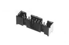
I will be using this type of connector in a male and female versions to incorporate any and all daughter to mother board connections. Suggestions are welcome as I am moving along. Thanks...
Attachments
It seems an excellent idea to have error correction & servo on a daughter board.Special acknowledgement to Damir for his setting me straight on the layout of the board.
I will be using this type of connector in a male and female versions to incorporate any and all daughter to mother board connections. Suggestions are welcome as I am moving along. Thanks...
It should be nice from you to post your "worst case reactive load model of a two way loudspeaker with crossover" schematic.Run a quick simulation of the amplifier driving the worst case reactive load model of a two way loudspeaker with crossover. Apply the worst case input waveform. Monitor the "OMG Something Is Wrong" current flowing in these simulated catch diodes. Finally, apply a conservative safety factor when spec'ing a real diode. Done.
It's not my schematic. It belongs to Douglas Self and Bob Cordell and can be found in their book(s) on the pages I indicated. Perhaps 30 minutes of internet search engine work might find the same or similar schematics online, in case your book collection is housed in another building.
Another way to answer the question "which real-world diode will I select, to perform the Catch Diode function" is to apply circuit reasoning. Think about properties of real-world (nonideal) diodes, and decide which ones are crucially important for the Catch Diode. And decide which properties are unimportant and/or completely irrelevant. Then use the Parametric Search function of a component sales website to find diodes which meet your requirements.
I imagine that some of the properties of diodes you might consider, could conceivably include (a) max reverse voltage; (b) max dc forward current; (c) nonrepetitive peak surge current; (d) capacitance; (e) leakage current; (f) forward voltage drop; (g) reverse recovery time; (h) package type; (i) price; (j) availability
A bit like someone to whom you are asking your way and who would answer you: "It's on the maps !" ?It's not my schematic. It belongs to Douglas Self and Bob Cordell and can be found in their book(s) on the pages I indicated. Perhaps 30 minutes of internet search engine work might find the same or similar schematics online, in case your book collection is housed in another building.y
A bit like someone to whom you are asking your way and who would answer you: "It's on the maps !" ?
Posting material from copyrighted sources (like Bob's book) is forbidden by general laws and DIYAudio forum rules.
So the "maps" are not free.
- Home
- Amplifiers
- Solid State
- Pizzicato, a 200W low distortion CFA amplifier