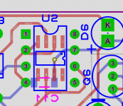
Cool !Layout pattern for the PNP 1381 and FZT957, it will be the same for the NPN
Layout pattern for the PNP 1381 and FZT957, it will be the same for the NPN The pink area is the soldering area for the tab on the device. The white is the solder mask. Please some comments for the sake of ideas or improvements or criticisms.And no I am not scared...Thanks
A word of caution. I don't know why you design your own footprint here, you probably have your reasons. But these footprints are normally as standard available in any layout software, and they have been developed and defined so as to ensure maximum reliability for soldering and use temperature gradients, heat sinking, and other factors.
So designing your own carries the risk of a non-optimum footprint, and should only be done if you absolutely know what you are doing.
Jan
May-be his software do not provide footprints that offer the compatibility between surface and through hole active devices ?A word of caution. I don't know why you design your own footprint here, you probably have your reasons.
...
So designing your own carries the risk of a non-optimum footprint, and should only be done if you absolutely know what you are doing.
The standard procedure in these cases is to take both, overlap them on each other the way you want, then generate the combined footprint. Different CAD apps have different procedures for it, so no universal way, but manuals/help file should explain how to do it.
For my Proteus I take 1st footprint, check Library|Decompose part, then take the other, again Library|Decompose part, then overlay one on the other, then Library|Make part. This also ensures pin numbering is consistent which prevents possible errors with connectivity later.
But as I said, with your CAD (KiCAD?) it probably is different.
Jan
Composite footprints can be tricky, if you overlap them it is a DRC package overlap violation in some cases. It can be generally ignored. Sometimes I make a special schematic symbol to address the pins that are involved, match the footprint but as Jan says every s/w has it's own ways of doing things and one s/w technique may not work the same for the other.
You would hope that the canned libs are fine, and error free so you will find out one way or the other, if you use them.
I can say all the ecad packages I have used and companies I have worked for, going back to Cadnetix's days, we never used the canned libraries for a number of reasons, imo they are usually incomplete/inaccurate, in some way or another. Usually cad libraries are designed for specific pcb and soldering manufacturing process in mind, but these days at least LPI solder mask is a standard. Lots of variables, you find out when you actually build up your design.
I do have to comment on this statement, I myself from experience as a layout designer do not put as much trust or faith in the canned libraries as Jan does but I have never used Proteus so I can not say for sure.But these footprints are normally as standard available in any layout software, and they have been developed and defined so as to ensure maximum reliability for soldering and use temperature gradients, heat sinking, and other factors.
You would hope that the canned libs are fine, and error free so you will find out one way or the other, if you use them.
I can say all the ecad packages I have used and companies I have worked for, going back to Cadnetix's days, we never used the canned libraries for a number of reasons, imo they are usually incomplete/inaccurate, in some way or another. Usually cad libraries are designed for specific pcb and soldering manufacturing process in mind, but these days at least LPI solder mask is a standard. Lots of variables, you find out when you actually build up your design.
Last edited:
Yes, sometimes it seems it's more an art than a science, but I wanted to sound a caution nevertheless.
One dual footprint I made by combining two existing is the DIL08/SOIC08 that we often use, see attached. DRC is not an issue with this.
Sorry Professor for hi-jacking your thread, I'll be silent again ;-)
Jan
One dual footprint I made by combining two existing is the DIL08/SOIC08 that we often use, see attached. DRC is not an issue with this.
Sorry Professor for hi-jacking your thread, I'll be silent again ;-)
Jan
Attachments
Last edited:
Some cad packages will not allow you to have duplicate pin numbers in a footprint, so another technique is required.
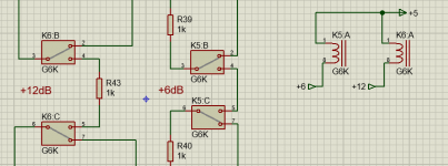
I am finding it convenient to tell KiCad that a certain DPDT relay (this one) is two separate components, each with its own PCB layout footprint and each with its own schematic symbol. One component is the coil and the other component is the DPDT switch. Then I place them on the layout in such a way that they interdigitate correctly and match the pin placements of the physical relay.
The more you look at the layouts, the more you see in which to improve upon. Even after I generate fab, I see things in the gerber viewer in which I can change. Boss/manager, used to say, enough is enough, push the "manufacture now" button. This is the art aspect of a layout, I assume that is why they had women do most of the layouts in the past. Now we have gerber viewers at the pcb fab, so even more checking, not like the old check plots/brown-line? days.
Maybe one day I'll give KiCad a go, to see how it ticks. Does it do cross highlighting/selection between sch and layout? 🙂
Maybe one day I'll give KiCad a go, to see how it ticks. Does it do cross highlighting/selection between sch and layout? 🙂
Last edited:
I am finding it convenient to tell KiCad that a certain DPDT relay (this one) is two separate components, each with its own PCB layout footprint and each with its own schematic symbol. One component is the coil and the other component is the DPDT switch. Then I place them on the layout in such a way that they interdigitate correctly and match the pin placements of the physical relay.
Yes; the better packages allow non-homogeneous parts. Even allow DPDT relays to be placed as two different switches.
Jan
Attachments
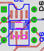
I am using Sprint Layout 6 by Abacom to do the layout. They had a macro for the smd SOT-223 in a library. I do not know if they developed it, or if I acquired it from AlexMM. He has shared a lot of macros and a lot of his work here on DIYAudio with me.
I took the device manufacturers suggested pattern on the data sheet and checked the distances between pads and the pad sizes. This is for the SMD device. I placed both of them on a board and reversed the macronization process of the FZT957 and of the PNP 1381. The 223 was very standard in relationship to the manufactures specs. I then enlarged the heat sink area of the 223, but left the contact tab solder mask alone as well as the other pads, and made the heat sink larger with holes for the double sided board. It may not and probably is not perfect, but I think it will work for our purposes. The only hole size issue is with the 1381, and I do not think that is critical.
The only issue I see is IF the devices in question here, need to be thermally coupled at some point. If they do, then it is back to the drawing board (screen) again and put on some 3D glasses and turn up the lights some more.
Basically, I am trying to get something that can be made and tested and working.
IF anyone has some suggestions, I am listening...😉
One way to thermally couple SMD/SOIC versions is to place one on each side of the board and stitch the heatsink areas together with a lot of thermal stitch vias.
Jan
Jan
Unless it is a common electrical point it would not work, the collectors are electronically connected to the Heat-tab. Maybe if they could be isolated electrically, with something. I think you are talking pancaking. Need some isolating syrup...
Yes, this matches my experience top, though I'm a novice in circuit design. I faced a second problem: the symbols could not have wires, and the footprints could not have tracks. I wanted to join some of the pads in a pre-decided way in my footprint itself, but couldn't do it because wires and tracks were not allowed. Jan, when you did the 8-pin composite footprint, did you put any tracks into the footprint itself?Some cad packages will not allow you to have duplicate pin numbers in a footprint, so another technique is required.
You mean separate in the schematic and a single block in the PCB layout? Yes, that's called a multi-part symbol in KiCAD, right?I am finding it convenient to tell KiCad that a certain DPDT relay (this one) is two separate components, each with its own PCB layout footprint and each with its own schematic symbol. One component is the coil and the other component is the DPDT switch. Then I place them on the layout in such a way that they interdigitate correctly and match the pin placements of the physical relay.
But KiCAD loses track of which IC's part B is supposed to go with which IC's part A. I have to go into "Edit Reference" and manually name each part of each multi-part component through a slow and laborious process to indicate the bindings. Eagle used to keep those bindings accurate very well, automatically. I just wish KiCAD's designers would use Eagle a bit and avoid making mistakes which others have already addressed.
The KiCad plot thickens ... slots & swapping, a good test for a tool set.
I am lead to believe that Sprint Layout 6 does not operate off a netlist, one with linkages to the schematic, that in a nut shell is very error prone and highly discouraged by me at least, for all but the smallest of connections & parts. I see them using it in the Apex thread, AlexMM is an expert, amazing what he can do with the error prone toolset. Still I would not recommend it, it makes your head spin, not in this day and age, you have better things to do than check to see if connections match a netlist.
If Mark is successful with KiCad, I would think it is better than Sprint if you want something for free. I know Jeff is using diptrace, he is successful with it. I thought it was not very good but I am picky.
At least Nigel does designs with his cad s/w
I am lead to believe that Sprint Layout 6 does not operate off a netlist, one with linkages to the schematic, that in a nut shell is very error prone and highly discouraged by me at least, for all but the smallest of connections & parts. I see them using it in the Apex thread, AlexMM is an expert, amazing what he can do with the error prone toolset. Still I would not recommend it, it makes your head spin, not in this day and age, you have better things to do than check to see if connections match a netlist.
If Mark is successful with KiCad, I would think it is better than Sprint if you want something for free. I know Jeff is using diptrace, he is successful with it. I thought it was not very good but I am picky.
There are coders and then there are layout folks, it seems that they do not talk to each other very much or get along very well 🙂 Does not take long to figure out, oh boy what were they thinking, do they design any pcbs with this stuff?I just wish KiCAD's designers would use Eagle a bit and avoid making mistakes which others have already addressed.
At least Nigel does designs with his cad s/w
Last edited:
I am probably going OT here, but can you explain what's wrong if your software doesn't support a netlist? Or is it the other way round?I am lead to believe that Sprint Layout 6 does not operate off a netlist, one with linkages to the schematic, that in a nut shell is very error prone and highly discouraged by me at least, for all but the smallest of connections & parts...
I've used Eagle, where one never needed to bother with netlists, and KiCAD, where it needs netlists. I haven't understood why software needs to be designed to use this intermediate representation called a netlist. My only hypothesis is that different groups of people wrote various schematic capture, sim, and PCB layout applications, and agreed to use a netlist as a common data format for making all of them work together. If a single team writes these applications, a netlist step is not needed.
Yeah it is off topic, we should start a new thread ... there are many reasons why the layout and schematic (netlist) need to be in synch. Who's is driving the bus comes to mind?
Last edited:
I don't doubt that they need to be in sync. I am questioning why an intermediate file called the netlist needs to be created. If the PCB layout editor and schematic editor can use each other's file formats, this extra step can be avoided. Eagle does it well, I feel. Its "forward and backward annotation" feature is really lovely.
- Home
- Amplifiers
- Solid State
- Pizzicato, a 200W low distortion CFA amplifier