If you want to put them (catch diodes), any 200V 3A or more diode will be ok ?
You can obtain the answer by (a) simulation, (b) circuit reasoning, or (c) another approach which you create. But it will take effort. Your effort.
Is-it allowed to promote commercial products like copyrighted vulgarisation books by the DIYAudio forum rules ?Posting material from copyrighted sources (like Bob's book) is forbidden by general laws and DIYAudio forum rules.
No comment 🙂Your effort.
BTW: We don't need those diodes, anyway.
Is-it allowed to promote commercial products like copyrighted vulgarisation books by the DIYAudio forum rules ?
Not sure what “vulgarization books” you are talking about, but advertising is not illegal and it is at the media owner (forum) latitude.
It may not be wise to omit a $0.50 diode, and instead pray that the four very expensive unobtanium lateral MOSFETS will not be damaged when a reactive load sends the amplifier output beyond the rails. Or, leaving it out may be an excellent micro-optimization of cost. Try it and find out the answer!
I had said this amp will be :Try it and find out the answer!
1 - Equipped with a very fast protection and silent stop: means output disconnected in µs before any power supply voltage will have time to decrease or any difference between input and output signal.
2- 2sk134 & 2sj49 are used in the simulation file because the models are available, but we gonna use 2sK135 & 2sj50. 160V, go figure. Not to forget the very high damping factor.
3- I use one amps with those MOS devices under +-75V since more than 30 years (recapped two times) and very high efficiency speakers (passive filters). Still waiting for your apocalypse (crossing my fingers).
But thank you for your philosophical advice. Yes, these diodes do not interfere, which is why I gave a positive answer to the question posed by Krisfr. Now, back to the topic, no need to kill a dead horse.
Last edited:
Tournesol, would you are anyone object to a SSR (Dual MosFet) being placed on the mother board and incorporated into the scheme of things? And I am including the Big Diodes on the board too.😀
kick the can down the road
Definition: INFORMAL•US
to put off confronting a difficult issue or making an important decision, typically on a continuing basis
Here it can be interpreted to mean: put the diode footprints on the PCB layout and then Somebody Else will decide, at a later time, whether or not to stuff and solder them.
Krisfr, watch your PM.Tournesol, would you are anyone object to a SSR (Dual MosFet) being placed on the mother board and incorporated into the scheme of things? And I am including the Big Diodes on the board too.😀
I took a little time to evaluate the Spladski proposition to cascode the input stage. I did not found any major improvement in slew rate or bandwidth or phase and gain margin: they seems limited mainly by the VAS. The only advantage I can see is that it can add more choices of various paired devices for the input stage, that could be of much smaller VCE. The good thing is it is just 2 resistors and 2 transistors added, with no other change, that could be by-passed on the printed board to match the simple V8 version ?
May-I add that our attempt to build a CFA with the rules of VFA (very high loop gain = low distortion) at the expense of slew rate and flat loop gain up to 10 or 20 KHz, does not exclude, changing components values (less gain, more local feedback both for input stage and VAS), to take an other politic with the exact same board and schematic, and to propose later, a more conventional CFA. Two different animals from the same printed board. In French, "Le beurre ou l'argent du beurre" ;-)
Attachments
If someone pull the ground speaker connector while amp is playing loud your output device is gone. 10A03 or similar SMT pleaseBTW: We don't need those diodes, anyway
Nice to see-you here, dimitri.If someone pull the ground speaker connector while amp is playing loud your output device is gone. 10A03 or similar SMT please
Do not worry, it's planned ;-).
(You are right, as usual, but take into account that the planned protection can disconnect the positive speaker connection in 6μS. Not fast enough ? ).
May-be it should be a good idea to put the protection diodes after the Mosfet relay ?
Last edited:
Lower Vf and lower Cj please, ideally with lower tRR if possible10A03 or similar SMT please
Mark, again, are you participating in this discussion to help, or to stretch your knowledge ?Lower Vf and lower Cj please, ideally with lower tRR if possible
If you have a better diode reference to advise us, be kind enough to indicate it as Dimitri did.
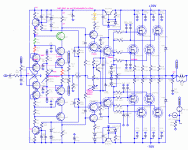
Krisfr, here a complete version of the amp allowing all options.
Optional parts only noted on the upper part of the schematic: bottom is symmetrical
In green, the resistance RC1 and the transistor Q5 to allow cascoded input stage for future developments.
Rci should be replaced by a strap, as well as collector to emitter junction.
In red, two resistances to reduce the gain of the input stage (degenerated emitter), could be replace by straps.
In orange, the two diodes can be by-passed to bring more latitude to Changes of the R27 value on the quiescent current of the VAS.
Caps C26, C28, C30 & C32 are optional to allow various damping of the Output transistors gates
Diodes DP1 & DP2, as requested, but, could be better after the protection right to the Speaker connector ? Place for them is an option in case someone want to play with the mos's nodes or dump oscillations due to parasitic caps.
What else ?
Attachments
Last edited:
I am suggesting possible optimization variables for your diode parametric search on DigiKey's website. Of course you are free to disregard, or invert, the recommendations offered.
After you have found three or four great looking diode candidates in a parametric search, you can use the wonderful octopart.com website to (a) find out which distributors have them in stock, and (b) to compare prices. There may be reasons why you prefer to buy from Element14, or from Mouser, rather than DigiKey.
After you have found three or four great looking diode candidates in a parametric search, you can use the wonderful octopart.com website to (a) find out which distributors have them in stock, and (b) to compare prices. There may be reasons why you prefer to buy from Element14, or from Mouser, rather than DigiKey.
Tournesol, can you make the very light grey parts lettering a darker color, ie Dark Grey or even black. Thanks for the final version. By the term Strap you mean Shorting or Jumper, am I correct?
Thanks Mark, please for the unwashed like myself, would you be so kind as to teach me how YOU would go about this device selection process, and just show me(us) how to do it. I am thankful of you willingness to share your concerns for the protection of the output devices. Thanks😎
Thanks Mark, please for the unwashed like myself, would you be so kind as to teach me how YOU would go about this device selection process, and just show me(us) how to do it. I am thankful of you willingness to share your concerns for the protection of the output devices. Thanks😎
I would kick the can down the road and let Tryphon Tournesol make the diode decision as late in the project as possible. In your position as volunteer PCB layout person, I would drop in a custom PCB footprint that accepts SMD + THT axial + THT TO-220 diodes. Giving him the flexibility to experiment with lots of different parts, in the real amplifier circuit, on the lab bench.
I was asking for your instruction, and or teaching. So your response is a lot less than I expected. But THANKS anyway. 😱
Please, excuse-me. I did-it for you can see better the schematic.Tournesol, can you make the very light grey parts lettering a darker color, ie Dark Grey or even black. Thanks for the final version.
Attached the V8 sim file that you can color following your preferences:
Tool -> color preferences-> components text.
The added parts have no value for the moment ;-)
Indeed.By the term Strap you mean Shorting or Jumper, am I correct?
Attachments
Last edited:
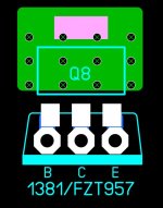
Layout pattern for the PNP 1381 and FZT957, it will be the same for the NPN The pink area is the soldering area for the tab on the device. The white is the solder mask. Please some comments for the sake of ideas or improvements or criticisms.  And no I am not scared...Thanks
And no I am not scared...ThanksAttachments
Krisfr, It is difficult for anyone to determine if your footprint is acceptable by looking at that .jpg, hole sizes, spacing, keepouts etc are impossible to determine. When you are done, if you load up/share the fab files, I can look them over in a gerber viewer which will allow me to measure and determine DRC, drill hole sizes etc. I will not determine if the layout matches the netlist. Another option for you is to load up the design at jlcpcb for a quote, you can then use their gerber viewer as a sanity check. Their viewer is just a quick check that your design loads okay. What cad tool are you using again?
Last edited:
- Home
- Amplifiers
- Solid State
- Pizzicato, a 200W low distortion CFA amplifier