What I posted is simulated and the negative has the same excellent
specs as the positive.
All readings are very "symmetrical" . 😎
OS
I had the op amp right the first time then. I changed it this morning.
Notice the grounding on didiet78's schema.
The stupid bypassed zener is also there ... 3 red led's are way less noisy.
They bypass the zener to compensate - stupid.
I could actually see the noise at the pass transistor with the zener.
My 5.4V led drop still gets the IC out to a 10V level for a 15V output.
OS
The stupid bypassed zener is also there ... 3 red led's are way less noisy.
They bypass the zener to compensate - stupid.
I could actually see the noise at the pass transistor with the zener.
My 5.4V led drop still gets the IC out to a 10V level for a 15V output.
OS
you can mitigate all that risk by using transformers with separate windings and just use two positive regulators.
🙂
mlloyd1
🙂
mlloyd1
Starting with schematic posted at #74 I build the current source around Q3 using a 2N3906 and a typical red led, I set the power supply at 20 volts and did get a 4.8 mA collector current.
It means that maximum current at the base of Q2 is 4.8 mA and if current gain of Q2 is 50 ( Q2 is a big power transistor ) maximum curreny of the power suplly is around 240 mA....
I did not build the diamond buffer but I think output stage will have a bias current around 100 mA, ..... 5 mA across R17 so 1.1 volt across R17 ... 1.1 volt accross R13 ... 110 mA at R13.
Will the power supply work with a 2 chanel amplifier ??
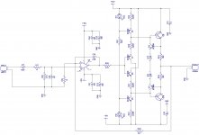
(below 1 ) is my best attempt at a "blameless line stage".
By "blameless" I mean ... these specs don't matter -
.5ppm and -210db psrr !!! (below 2/3).
The Jung super reg was a "beatch" , it oscillated on some op-amp
models and not on others ... as it was originally published.
So , I treated it as a feedback amp , broke the loop - and optimized
it for phase margin and bandwidth. In doing so , I had to compromise
between performance and stability (like in my amps). 😉
My Jung did not have the LF PSRR of the original , but had superior HF
performance ..... added a CRC instead of that LM317.
In the end , I have the Jungs performance , add my line stage for
that -210db pssr ... plus ,ANY IC will work ! (in either PS or amp).
"Roll yer' chips in my designs !! 😀
Edit - this is for analog ... for digital , a mosfet reg. is the way (noise performance).
OS
OS, naturally I am interested in better compensation of the Jung reg! Looking at your schematic I can't see any specific comp parts (except maybe the base stopper for the series device).
What specifically did you change?
Jan
OK , first I read this ... Op-Amp Based Linear Regulators
The four issues were -
1. startup
2. some op-amps would oscillate.
3. picky about input/output capacitance (or no load).
4. picky about choice of reference.
I hate circuits like this , and am willing to sacrifice some
performance for a better "idiot" factor.
Start-up with the zener added noise.... Yuk ! (3 red leds)
The oscillation - I broke the error amp's FB loop and checked the margin
with just about all of LT's op-amp models. Some were close or over 180 dg.
at various frequencies.
So, I started omitting parts ( those 4 - 120u caps).
I lost 20db PSSR (-140db jung vs -120db /mine). What I gained
was 30+ to 100 dg. margin from .1hz to 100mhz - any model/any load.
(and any output capacitance).....
So we have a "jung lite" that will be way cheaper to build. Sorry to
blasphemize the original , but when any model for any device and
any load give me oscillation free operation - I go with it (and it
usually works better than simulated).
PS - my expected load is .4A for my line stage app.
Below is what will be built. simulate it ....swap out any major
device - perfect !
Edit - the 100pF caps eliminated the one "close call" phase margin
region (>2mhz).
Edit 2 - much higher Z for the error amp inputs really made a difference ,
as well. (more margin still).
OS
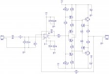
Attachments
Last edited:
Starting with schematic posted at #74 I build the current source around Q3 using a 2N3906 and a typical red led, I set the power supply at 20 volts and did get a 4.8 mA collector current.
It means that maximum current at the base of Q2 is 4.8 mA and if current gain of Q2 is 50 ( Q2 is a big power transistor ) maximum curreny of the power suplly is around 240 mA....
I did not build the diamond buffer but I think output stage will have a bias current around 100 mA, ..... 5 mA across R17 so 1.1 volt across R17 ... 1.1 volt accross R13 ... 110 mA at R13.
Will the power supply work with a 2 chanel amplifier ??
The Hfe @ 1V is bad. 20V is 120 (see datasheet).
The simulator shows the D44/45 "running out of gas" at about
a 700ma load.
Use a tip 147/142 for 1.5A. (just simulated a BCxxx/D44 pass device combo).
Or, raise the CCS current.
OS
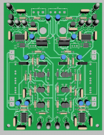
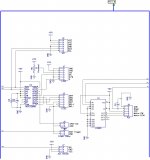
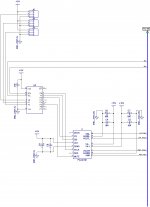
Here's a reworked version of the linestage and regulators. Q3 & Q4 mount under the board on the chassis. J1 is the regulated output connector. I don't like it. The power traces to it are way too long. I'm thinking .100" pin headers at the regulator caps might be a better choice. I could change to two euroconnectors as well but then we need to be careful we don't cause ground loops when we use the connectors.
Attachments

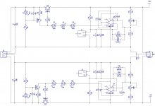

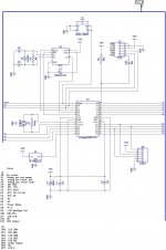
Here's the I/O selector board to date. Again this is a reworked version of Linuxwork's design. I've added a PGA2310 digital pot instead of his stepped attenuator. That looked like way too many relays.
It has three rear panel RCA connectors and an input for the DAC. It also has relay controlled line out and headphone outs. This can be modular and select 10 more ins and outs but for my application 4 inputs is probably three more than I will use.
I think the logical choice would be to add the digital inputs to this board and either add the DAC to this or make this a backplane for the DAC. I'm open to suggestions before I start laying out this or the controller.
Attachments
First off I am not thrilled to review your design because I do not want to look as if I am being overly critical and I would have none it differently, as I have provided you my ideas for a pre-amp design already.
I can think of a few(lots) of ways to reduce costs, complexity, pcb area. screams for a 100 pin xmega128a1. i do understand where you are coming from the unknown of the code aspect.
have you considered adding a FM radio for the meager cost of
https://www.sparkfun.com/products/11737
i have this code all running and for free, it fills a m328. Actually the author, who offered the code for free ran out of space on a m328, so I continued with his code and ported it to xmega, as I have tons of code space for enhancements.
one thing i see really weird is why are you going to use i2c to make a spi bus, for the pga2320? it offers no more digital isolation and just makes for more complicated coding and slows down the write op unnecessarily. i have this code already written and running in bascom.
but it sounds like you are a ardunio/c fan, so what can I say.
stuck with a 32 pin package m168/m328! do you have any idea how much code you actually need for the h/w features?
Last edited:
First off I am not thrilled to review your design because I do not want to look as if I am being overly critical and I would have none it differently, as I have provided you my ideas for a pre-amp design already.
I can think of a few(lots) of ways to reduce costs, complexity, pcb area. screams for a 100 pin xmega128a1. i do understand where you are coming from the unknown of the code aspect.
have you considered adding a FM radio for the meager cost of
https://www.sparkfun.com/products/11737
i have this code all running and for free, it fills a m328. Actually the author, who offered the code for free ran out of space on a m328, so I continued with his code and ported it to xmega, as I have tons of code space for enhancements.
one thing i see really weird is why are you going to use i2c to make a spi bus, for the pga2320? it offers no more digital isolation and just makes for more complicated coding and slows down the write op unnecessarily. i have this code already written and running in bascom.
but it sounds like you are a ardunio/c fan, so what can I say.
stuck with a 32 pin package m168/m328! do you have any idea how much code you actually need for the h/w features?
I'm just kicking around different ideas at this point. As I mentioned earlier I would like to keep my preamp simple. Just an input selector and volume control. Others are welcome to do whatever they like.
This type of display module also looks like an easy solution to some projects I've been meaning to get to in my shop. For example I need backgauge controllers for my shear and brake. Mine are dinosaurs and both packed it in. I've been using a tape measure for a few years now.
All this will work on an Arduino. Linuxworks already has it running on his LCDuino and has DIY boards already available. The LCDuino-1 display I/O processor
add to that
the portable design uses a xm192a3 in the 68 pin tqfp(0.8mm), since it is the series to have the largest flash. even then I ran out of pins and needed to use a pca9555 i/o expander for the leds.
I am not aware that linuxworks "bryan" has released any of his code to the public. he also recommended using the cs3318 as well since he had pga2311 latchup in his mach up, but could not determine if it was his layout, which is a possibility. I had some conversations with him, a nice guy, he helped explain a few things for me, i have his email.
sure I understand bryan "linuxworks" and his partner "ABM" are trying to make a buck, so sure, go for it if you want to support him, use his h/w but you are stuck with his code and h/w, because the h/w & s/w go hand in hand and the source code is IP.
simple is good too, but what i see in your design is over complication too.
My code, h/w progression,
1) Elektor high-end preamp using pic and pga2311
2) a sparkfun xm128a1 breakout pcb and added that to a protoboard to make my dev proto.
3) fully blown radio/media player stereo receiver. 40-50 Kbyte of code.
you can have one h/w base and have tons of s/w possibilities.
bryan is a much better coder than i, he is a pro, i am a hacker, so "c" is his natural language.
I am looking at arduino, right now, all i see is a big degree of unnecessary complication. but because ardunio is gcc based it has the horse power behind it.
Either bascom or gcc or asm, they all do the same thing at the machine code level. it comes down to how much time you want to invest in it.
I reviewed danzup/alex MM designs, real simple stuff, all or most done for you already.
it is in two (edit 3) zips, take a look, some complete designs in zip files.
Attachments
Last edited:
Hey guys , chill !
I would just be satisfied with a analog volume control / buffer /DAC.
I use my PC 99% of the time.
The digital is just "icing" on the analog cake.
Which means it can be simple , too.
OS
I would just be satisfied with a analog volume control / buffer /DAC.
I use my PC 99% of the time.
The digital is just "icing" on the analog cake.
Which means it can be simple , too.
OS
Here's a reworked version of the linestage and regulators. Q3 & Q4 mount under the board on the chassis. J1 is the regulated output connector. I don't like it. The power traces to it are way too long. I'm thinking .100" pin headers at the regulator caps might be a better choice. I could change to two euroconnectors as well but then we need to be careful we don't cause ground loops when we use the connectors.
J1 can/will be used for local +/- 5v (further regulation) at a DAC or attenuation
PCB. So , longer traces will be no issue with local decoupling in that case -
it will feed wires !
That layout looks real good , similar to the better PCB kits I've seen.
OS
Hey guys , chill !
I would just be satisfied with a analog volume control / buffer /DAC.
I use my PC 99% of the time.
The digital is just "icing" on the analog cake.
Which means it can be simple , too.
OS
I'm the same. Big flashy screens and blinking LEDs are too much of a distraction. It's nice not having to get up to adjust the volume though.
- Home
- Source & Line
- Analog Line Level
- Pitchfork pre-amplifier