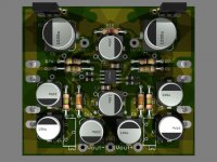
Sorry, I was fighting with eagle, still a little oops on the silkscreen but here is the other side. I also have an inbetween version with dip opamp....
It still needs a few spots of spit, but I was so eager to show you.
It still needs a few spots of spit, but I was so eager to show you.
Attachments
Last edited:
It certainly shows promise. Here are a couple of things you might want to think about:
- there is no way to secure the boards to the chassis, and the fuse caps are exposed...
- too many jumpers for such a simple circuit, consider a double sided layout.
- given the difficulty dealing with SMT components, is the reduction in size they give you really necessary?
- on a similar theme, there are no prizes for compressing a circuit into the smallest area- it doesn't sound better, it's hard to put together and harder still to work on - it's worth giving serious thought to how small you really need things to be.
- traces at acute angles on printed circuit boards are UNCOOL.
- components should not be mounted on the underside of the board, it's bad practice. Sometimes it's unavoidable, but when it can be avoided it should be.
/R
Last edited:
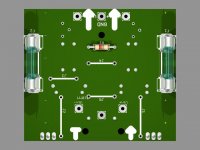
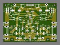
Hi, on the top (well, bottom) view you will see 3 black dots, this is where standoffs screw into the board, the idea was to make a bottom pannel for accessing the fuses... might be alot of work, and they may still move to the top as there is about 15mm available on the case I am designing it to go into... thats normally where I start getting a feel for the size of things. First I wanted to get it no wider than the transformer.
The SMT caps are a bit of an experiment, there are through hole caps with slightly higher specs, but these are the nicest ones I could find in terms of low noise, max ripple and price, they are from panasonic.
The 100uF caps are FC series, manuf. part # EEEFC1E101AP good for 450mA ripple and 0.3ohm impedance at 100kHz, size F.
The 1000uF caps are from the FP series, EEEFP1E471AP, 1190mA, 0.06ohm and size G.
I.e. in both cases they could be replaced with throughhole components as there is quite a range in that size limit.
I agree on things getting harder the smaller it gets, but to me its part of the challenge. Also I am normaly (lol, always) financialy stretched so the smaller the PCB, the smaller the case, the smaller the bill. Part of why that one resistor still lives on the wrong side of the board. I also tried to get traces, especialy those around the 4 input pins as equal and short as possible, getting a scope at the end of the month I believe, so then I can play around more with diffirent lenght traces etc, while haveing the vehicle to measure and learn from it. For now, shorter is better in my book (with much respect to your viewpoint)
Yep, I know there are some acute angles left, part of the spit and polish I mentioned, but I have rounded most curves to the max space allows for. You will also notice I placed the input ground a bit further up the middle trace, so that the grounds from the Transistors aproach it from the oposite side of the ground returns from the chip, I also wanted to route the ground out around to it as well so the chip doesn't have to share the ground return path of the output, but that would make the return path too long and would probably be a worse compromise than what I have.
Sadly the only way to get high tollerance,appart from buying many and haveing a good meter with good repeatability, is to use SMT for those resistors, technicaly I could use 0806 in those two spots as the parts are available and about the same price, the 03's just seemed to fit better, and I'm quite used to tacking those on, even with a soldering iron, (I cheat and use reflow solder).
The 5 jumpers are a result of the oposite orientation I got when switching to the SMT chip, I don't think they justify the cost of a dedicated layer though. Especialy as I'd like to get the PCB's manufactured and soldermasked etc... for the sake of being pretty. I guess I try to marry what is for me an artistic layout with the best of my little knowledge of electronics, most learned here, the rest made up by my ego.
The choice of schematic, well thats the part that shows my veneration and enjoyment for the VSP that you designed and serves me so well.
What do you think of my choice of chip?
I'll compare some specs to opa2132
OPA2211
VOLTAGE NOISE: 1.1nV/√Hz at 1kHz
OFFSET VOLTAGE: 150µV (max)
SUPPLY CURRENT: 3.6mA/Ch (typ)
oPENLOOP GAIN 130db
OFFSET VOLTAGE DRIFT: 0.35µV/°C (typ)
SLEW RATE: 27V/µs
CMRR 114db
OPA2132
VOLTAGE NOISE: 8nV/Hz (1kHz)
OFFSET VOLTAGE: 500µV (max)
Iq max 4.8mA/ch
OPEN LOOP GAIN 120db
OFFSET VOLTAGE DRIFT: 2µV/°C (typ)
SLEW RATE: 20V/µs
CMRR 100db
Using a double-sided board will do far more for the sound quality than fussing over capacitor datasheets. You get a ground plane, lower noise, more stability, the remaining traces simplify and in many cases shorten, and there is no need for jumpers or convoluted layouts. The crosslinked nature of the Xreg circuit means that it does not lend itself to single-sided layouts. I managed it, (note: no jumpers) by being sneaky and lucky at the same time.
Saving a couple of bucks for shaving 1-2 square inches off the board, or not including a second layer - this doesn't make sense in the face of the large fixed fabrication costs on a small run of private-use boards, and certainly not considering the total cost of the project. Likewise the few cents saved on SMT cannot be justified given the total costs of building DIY audio.
A through-hole component can be reliably soldered in place in under 30 seconds, no tweezers or magnifying glass needed. SMT is a total pain unless you are fully set up to deal with them - a considerable expense in time, tools and equipment.
Of course, you will do what you choose to do. My advice however is that you start again from 4x the board area, standard mounting holes at the corners, and put all the parts on the top layer. Find a nice, sensible, clear layout, then resize the board to fit, not the other way around.
PS: Your choice of opamp is very fine, rail-to-rail is an advantage as the headroom is increased (Vout can get closer to Vin)
PPS: What CAD software did you use to render the board?
Last edited:
Sadly double sided is not an option currently, the costs for the PCB nearly doubles because of the high setup fees, the actual board itself is not so much more, just the setup bit....
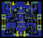
Ok, so I had some time and thought I'd go at it from a fresh start. There is now only one jumper left, which in theory I can remove easily by just turning around the transistor, but then I loose the simetry of the layout over their heatsinks...
Also the 2 220R resistors are hiding on the back of the board, but they were placed useing front position, so for those who do not care for the look, the space is allready there to just put them in from the front.
I have been doing a little bit of SMT, and sure, if you were to do large boards with lots of parts it gets troublesome without a nice setup. I don't see major problems with the 5 smallish SMTs on the circuit though, bite your tongue in the corner of your mouth, use a bit of tacky flux and its no problem.
Overall I guess the layout is slightly cleaner now than my first go, I am pretty happy with short paths to the respective caps for each point,, appart from the one 100uF feeding the chip's one rail... there is a number of things I would have liked to see diffirently about it, but once again, it seems like the smallest compromise between all my personal priorities.
Oh yea, I use good old povray after exporting the boards useing the eagle3d ulp script from eagle.
Ok here is the board, what do you think?
Attachments

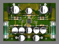
Looks better, though there are still several things I'd file under "bad practice".
I should say that I don't have professional experience in board design, I'm mostly going with the recommendations of Olimex, and what I've seen done on commercial audio equipment and research equipment I've pulled open.
- Components, traces, and lettering should not run to the very edge of the board.
- Mounting holes for standoffs should be at the corners, with plenty of clearance.
- Component names on the silkscreen should still be visible after the component is soldered in place.
- It should be possible to replace a component without removing or damaging other components. Now look at your board and imagine you want to replace C3. You'd have to remove all four electrolytics nearby just to get at it!
- Heat generating components, Q1 and Q2 should not be butted up right next to components that derate with temperature like electrolytic capacitors.
/R
I agree on space required on edges, currently the issolataion edge is well over a mm, but it is not too much of an issue for me, as the board will have side edges to slide into slots in an extruded case. It should definately get a little extra edge at the output side of things.
The nylon standoffs I normally use when mounting to a bottom panel, would fit well enoug as there is nothing on the other side of the board near them, but as I said, it is actualy going to slide into slots, I'm not realy sure what secures the boards in the slots, will have to see when I get the cases. The holes did move out quite a bit to the corners, in between our two posts.
Yep on the silkscreen issues, what you saw were artifacts of a quick job, was hopeing to catch you online... not saying it is perfect yet, but there has also been some improvement.
Yep, replaceing parts may indeed be harder than with throughole, I can not argue counter to that. Part of why I am choosing higher quality parts than the cheapest available, I guess I could buy all the caps for under $4, probably much less, if I went for cheapies. appart from voltage, no component is brough close to its operating limits as far as I can see.
Do you think a scope would be enough to see diffirences in noise floor etc. from things like lead traces etc. I'm quite willing to build two versions to compare things from a measurements point of view.... well that, and I want to learn how to use a scope properly.
My thoughts are with you over there, I imagine things must be quite tough at the moment.
I hope there will not be too much heating on the transistors, as I will only be powering a 50mA 12 or 15V (if I can reach it) opamp, appart from the opamp on the PSU itself. I expect about 0.5W of heat dissipation over there, should be fine with the 105C caps there. I am very religious when it comes to placeing bypassing caps as close to the point where I want them to perform their job, and will most of the time prioritise this over other factors.
You may also notice more trace pours than before as I wanted nice low impendance traces.
There is provision for two small 0.8A bridge rectifiers, but I also left holes to connect standalone rectifiers.
Attachments

Last edited:
Your layout is fundamentally cramped. That may be a problem for you or it may not be. You'll have to find out for yourself.
There are still a couple of weird things with the board, small unmarked components near the GND, and curious, unmarked pads above C9 and R7A. The inputs are unmarked.
It's fine for personal use though.
re. spotting differences in board design on a oscilloscope: pretty much forget about it. Any spurious noise above the noise floor of the op amp is going to be most likely noise pickup on the test leads. You'd have to be very rigorous in your test setup to be able to spot any difference.
Hi there, yes, I am going for cramped (high density layout), its a matter of personal taste and of coarse fitting the enclosure I want to use.
The mystery pads are as follows, 10mm wire jumper running north to south above R7A, the pad above C9 is for GND in... don't ask 🙂
and slightly above R7 is the one 220R, as you can see it can be applied on top of the board, sam thing just left of the IC, with the other 220R. I just think it LOOKS better with them on the other side, plus I don't figure they will ever require servicing. The life cycle of parts around my house is normally only until a better brighter design looms and parts donors become required.
It is only for personal use, I would not feel right useing your work as is for commercial purposes. I want to make two of them, one small one for my DIYed L/C meter, which basicaly runs a small pic a small comparator and 1x16LCD, and something more boutique for my phono amp's chip. A VSPS with OPA2228.
Oh yes, the mystery parts close to ground are two 0603 status LEDs and resistors to drop the voltage for them. I might still change this to 1 LED and resistor from V+ to V- as some believe there are less issues with that way of applying an LED.
Last edited:
Hi, after two years I have some time and need for improvements.
Changed from Frog to DL304 so needed some more gain.
Also bought some mica caps and orange drop for C1 and C2.
After reading the two complete threads I wonder if I should go for C3 inside the feedback-loop or leave it as it is.
Since it's not on the official PC3 I guess it's not worth the trouble?
I'll need an extra piece of wire between the C3 output and C1 and C2, maybe this will pick up hum and RFI?
Well, I finished it today and it sounds very impressive.
Sound is more coherent, more foottapping, but also cleaner mids and highs with no more smearing on the esses.
I also got rid of some hum.
Of course not only from putting C3 in the feedbackloop but also by replacing C1 an C2 with orange drop/silver mica. And put it in a bigger box with better cinch-parts and I moved the V++ and V-- lines away from the PC. Before they were going under the printed board, now some cm's nect to it. And because of this it was possible to get the earth-routing better. From COM to left Xreg to left PC and same for right.
Before Xreg and PC were starred to COM, so no direct earth-connection between Xreg and PC. (Was to difficult in the crammed space)
Yesterday only one channel was working and it had a little problem with a german radiostation. After repairing the other channel no more radiosounds. Keep my fingers crossed!
I bought the Phonoclone 3 boards a while back from RJM. But have been sidetracked by helping to develop a cheap easy to build DIY MM stage that runs on batteries.
Another reason I didn't jump in was I don't have a LOMC cart, having ordered one months ago but because of the problems in Japan it hasn't arrived yet. I have a nice Benz Micro Ace HOMC cart that I love.
Well I decided that the Phonoclone 3 may run on batteries I also thought that using the gain calculator provided by RJM I may be able to use it with my Benz Ace.
It has a resistance of 90 ohms and an output of 2.5mv's. Then I created a design with my PCB design program and etched a board for it, with both channel on the same board sharing a ground rail.
I just completed it and am amazed at the results, the noise is low very low, lower than my Cambridge Audio 640P which has a discreet front end.
I used the OPA27gp op amps as recommended, the 1nf caps are just Nichicon Metalized Plastic Films and I used all metal film resistors, even though I did buy the carbon composition ones. I added a 0.1uf poly cap to each 100uf filter cap, for lower noise.
I have R1 at 100 ohms and R2 at 300 ohms and the gain is perfect. I am using two 9v alkaline batteries in series to run it with the center connection as the ground.
Whatever I did it's worked out fantastic, I can't wait to get my LOMC cart to try that out with it. I only have to alter R1 & R2 to suit.
It sounds great already right out of the blocks, it has a smooth, warm yet detailed sound, it will get better as it breaks in.
Well done RJM, this is a fine project.🙂
Here's a nude pic of my homemade PhonoClone 3, I will have to build it on the supplied PCB's next.
As a follow up for those trying batteries or different op amps, adding a 0.1uf ceramic capacitor to each 100uf filtering cap helps with noise and oscillation IMO.
I can crank mine right up and it's dead silent, no noise at all, it even makes my modded CA 640P's sound noisy by comparison.
Also trying a 33pf poly cap across R2 should help as well while not limiting the bandwidth.

I can crank mine right up and it's dead silent, no noise at all, it even makes my modded CA 640P's sound noisy by comparison.
Also trying a 33pf poly cap across R2 should help as well while not limiting the bandwidth.
Hi, quick newbie question on installing the opamps and sockets. I realize that you solder the sockets in first, but after inserting the opamps into them do you need to solder the opamps into the sockets?...I don't think you do but want to reconfirm.
Cheers,
Kirk
Cheers,
Kirk
sockets are meant to enable changing the amps without soldering
Which leads to "opampus-rolling-itis" an incurable disease who's symptoms can only be relieved by trying out different op amps, sometimes on a daily basis.😛
- Home
- Source & Line
- Analogue Source
- Phonoclone 3