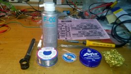
With SMD soldering the challenge I find is in not using too much solder. I only rely on the flux in the solder itself but that burns off very quickly - perhaps I'd do better to use additional flux on all components as I do on very fine pitched parts.
Thanks for the feedback on the sound - yes its one of the puzzles of developing DACs by ear to distinguish between what's caused by the DAC and what's on the recording. Only playing a wide variety of recordings I find can help with determining that. Ultimately though its down to satisfaction from the music and not being distracted by some characteristic brought into that by the DAC.
Thanks for the feedback on the sound - yes its one of the puzzles of developing DACs by ear to distinguish between what's caused by the DAC and what's on the recording. Only playing a wide variety of recordings I find can help with determining that. Ultimately though its down to satisfaction from the music and not being distracted by some characteristic brought into that by the DAC.
...l hear random low level noise such as switching on and off individual tracks in a multitrack recording...
Please, which specific record and track did you hear this? I would be curious to try to hear it.
//
It really helped me a lot in soldering the SMD parts when I used thin soldering wire.
0.5mm solder and 0.5mm tip on the soldering iron.
I applied flux paste with a small brush on the PCB pads.
I find it easier to solder the ICs first, then the transistors, then the resistors and capacitors.
George
0.5mm solder and 0.5mm tip on the soldering iron.
I applied flux paste with a small brush on the PCB pads.
I find it easier to solder the ICs first, then the transistors, then the resistors and capacitors.
George
Attachments
TNT. The random noise are artefacts which is no longer audible after upgrading firmware and change of usb cable.
My lead solder is 0.8mm and standard Goot soldering tip that is too big. Usually there is too much solder on a big tip and l have to suck it up the excess
Phidac sound reminds me of a Denafrips dac sound. After the pandemic is over, l will arrange a direct comparison
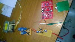
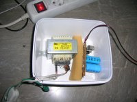
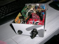
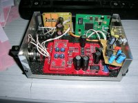
I set up this PSU for the PhiDAC hex from parts I had.
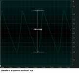
I wound the common mode choke. 3.1mH, 45mOhm. 17turns bifilar winding of 0.38mm enamel wire over a toroidal ferrite core (12.5mm OD, 7.7mmID, 6.4mm height)
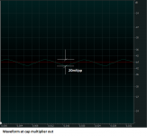
The cap multiplier is a left over from some old project (probably for an JLH headphone amplifier).
The LM317 voltage stabilizer is Elvee’s brain child: D-Noizator: a magic active noise canceller to retrofit & upgrade any 317-based V.Reg.
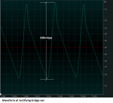
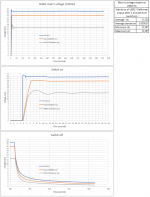
Static measurements of the whole PSU look good.
George
I wound the common mode choke. 3.1mH, 45mOhm. 17turns bifilar winding of 0.38mm enamel wire over a toroidal ferrite core (12.5mm OD, 7.7mmID, 6.4mm height)
The cap multiplier is a left over from some old project (probably for an JLH headphone amplifier).
The LM317 voltage stabilizer is Elvee’s brain child: D-Noizator: a magic active noise canceller to retrofit & upgrade any 317-based V.Reg.
Static measurements of the whole PSU look good.
George
Attachments
-
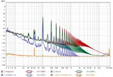
 10-FFTs of LM317 DeNoiser and shorted probe.jpg151.9 KB · Views: 184
 -
 9-combined FFTs (REW).jpg187.1 KB · Views: 161
 -
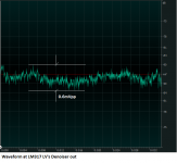 8-LM317 DeNoizer out-zoom.png47.9 KB · Views: 146
 -
 7-capacitance multiplier out-mV.png16.2 KB · Views: 145
 -
 6-coil out-mV.png33.1 KB · Views: 149
 -
 5-bridge out-mV.png37.5 KB · Views: 156
 -
 4-varying mains.png70.4 KB · Views: 477
 -
 3-stable mains.png58.2 KB · Views: 491
 -
 2.jpg517.8 KB · Views: 510
 -
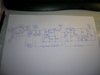 1-schematic.JPG619.2 KB · Views: 518
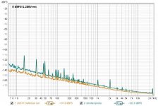
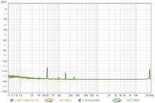
The two FFT plots in the previous post seemed a bit suspecious to me.
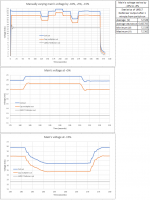
The testing chain was: 100MHz (x1) probe, into an Hameg 203-7 oscilloscope. The Y out of the scope into the M-Audio USB Audioplile soundcard, then reduction of the gain (-14.073dB) in Audacity to compensate for the increased gain of Y out. I noticed that smoothing in REW’s RTA plays some tricks in the vertical scaling.
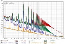
I run the test again. This time the testing chain was: 100MHz (x1) probe, into my AD620 test preamplifier in (x1) single ended configuration, then AD620 output into the M-Audio USB Audioplile soundcard.
FFT plots vertical scaling is proper now.
George
The testing chain was: 100MHz (x1) probe, into an Hameg 203-7 oscilloscope. The Y out of the scope into the M-Audio USB Audioplile soundcard, then reduction of the gain (-14.073dB) in Audacity to compensate for the increased gain of Y out. I noticed that smoothing in REW’s RTA plays some tricks in the vertical scaling.
I run the test again. This time the testing chain was: 100MHz (x1) probe, into my AD620 test preamplifier in (x1) single ended configuration, then AD620 output into the M-Audio USB Audioplile soundcard.
FFT plots vertical scaling is proper now.
George
Attachments
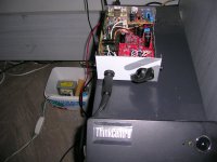
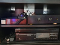
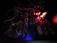
First public appearance of the test-run (industrial design disgrace of the year)
Nevertheless, they all work together harmoniously 🙂
George
Nevertheless, they all work together harmoniously 🙂
George
Attachments
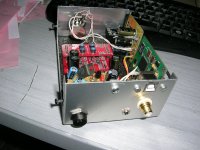
What is the function of the switch on the board?
Further listening reveals that this dac is a soundstage champion. Music envelops you.
resonance decay in piano , string instruments is very good.
it out do another TDA 1543 with diy paradise output stage .
Further listening reveals that this dac is a soundstage champion. Music envelops you.
resonance decay in piano , string instruments is very good.
it out do another TDA 1543 with diy paradise output stage .
Was using a cheap chinese xmos board sound was pretty good ..switched over to a jlsounds is2overusb .. holy sh*t wow
What is the function of the switch on the board?
Hi Wong - its a digital phase switch. The DAC's normally non-inverting (true phase) but if you flip that then it becomes inverting. Note the TDA1387 chip itself is inverting, presumably because its recommended to use it with an opamp I/V stage which inverts.
Thanks for the feedback @Dingo Dingo, @kp93300 and @r8833. The JLSounds interface is an isolating one? If so that normally makes a significant difference.
Was using a cheap chinese xmos board sound was pretty good ..switched over to a jlsounds is2overusb .. holy sh*t wow
Hi r8833
I am thinking of getting the jlsounds unit.
What configuration is it needed (Pin 5, 6) for working with PhiDAC?
Do you use it with the two external PSUs ?
George
George,
I think thats a picture of a older board. I have a V3 board
on my JLS board I left pin5(A1) and pin6(A6) alone.. didnt use.
On V3 board there is 20 pin header
pin 11 (BCLK_I2S) > clk
pin 13(DATA_I2S) >data
pin 15(LR_CLK_I2S) > ws
gnd >gnd
jumpers on B1 and B2
Rich
I think thats a picture of a older board. I have a V3 board
on my JLS board I left pin5(A1) and pin6(A6) alone.. didnt use.
On V3 board there is 20 pin header
pin 11 (BCLK_I2S) > clk
pin 13(DATA_I2S) >data
pin 15(LR_CLK_I2S) > ws
gnd >gnd
jumpers on B1 and B2
Rich
Thank you Rich
I see. The new configuration has different settings J1 to J4 and B1 to B5 (more complicated)
http://jlsounds.com/uploads/I2SoverUSB v.III.pdf
Which drivers did you use from the list (assuming Windows)?
Drivers - I2S over USB Audio
George
I see. The new configuration has different settings J1 to J4 and B1 to B5 (more complicated)
http://jlsounds.com/uploads/I2SoverUSB v.III.pdf
Which drivers did you use from the list (assuming Windows)?
Drivers - I2S over USB Audio
George
- Home
- Vendor's Bazaar
- PhiDAC hex kits with pre-built filters