Re: Re: Re: Re: Re: Re: fighting VAS
It depends on your point of view. If you see the resistor as an output load of the LTP, than the gain of the LTP is reduced. OTOH, if you see it as input shunt of the VAS, than the gain of the VAS is reduced.

Edmond.
G.Kleinschmidt said:
Well technically it’s the voltage gain of the LTP which is reduced
................
Cheers, Glen
It depends on your point of view. If you see the resistor as an output load of the LTP, than the gain of the LTP is reduced. OTOH, if you see it as input shunt of the VAS, than the gain of the VAS is reduced.
Edmond.
Bob Cordell said:
I think that the key thing to keep in mind here is that the amplifier should not clip or misbehave when briefly called upon to deliver a peak current that could correspond to a 1 ohm load. That is indeed a lofty goal, and need not always be realized.
Based on reactance and stored energy, it is in principle possible for a loudspeaker, when driven with the right waveform, to demand considerably more current than would be predicted by looking at its minimum impedance. This can, in principle be by a factor of two or more. It is probably rare, but should be kept in mind. This is a big part of the idea behind so-called high current amplifiers. Otala studied this and there is also information on this in my IIM paper at www.cordellaudio.com.
This is not to say that the amplifier even comes close to meeting its normal distortion specs during that brief burst. If you can handle a 2-cycle tone burst into one ohm without clipping or blowing up, you are pretty much there, in my opinion, even if the distortion would be a huge 0.1%. You do not want the amplifier to lose control of the speaker under these conditions.
For a 100-watt, 8-ohm amplifier, this might translate to a 40-amp peak output current capability. With three output pairs, this would mean about 13 Amps per device. You may not be far from being able to do that briefly with those devices if you have enough gate drive. That is certainly possible with the verticals I am familiar with, but I must admit that I usually shut them down at about 10A per device for anything other than a very short duration event.
Cheers,
Bob
Something as simple as a R-C network will do this. Use a resistor corresponding to Re and a small cap compared to the frequency and give it a full power square wave 🙂 The peak current will be like 3-4 times that of an 8 ohm resistive load.
I did an experiment where I tried destroying a lateral mosfet if you are interested, post 1, 9 and 10:
http://www.diyaudio.com/forums/showthread.php?s=&threadid=111116
I failed. 😀
Sure (especially in a combo amp ;-)... I just wanted to point out that the effect exists...jcx said:one could comment on the irony of being concerned about cap microphonics in tube amps...
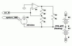
Something like this (see attachment)?[Distortion measurement resolution was extended by using Graeme's method of grounding the positive amp input and driving the xfmr isolated pwr amp's gnd with the signal source.
The negative amp input/feedback node was amplified by 30x with a opa228 "gnded" to the positive pwr amp input/measurement ground.
This gives a single ended amplified version of the error V at the pwr amp's input [...]
- Klaus
Attachments
looks right, "removes" the test signal components - actually they still appear in the input error V but are reduced by the amp loop gain at the test frequencies so you are mostly looking at the distortion residual when used with high loop gain amps
the test signal reduction means amplification can be used between the error V and the the soundcard input to extend effective dynamic range
I found that my standard EI power xmfer had <20pF pri-sec Cap, you could add a external isolaton xfmr in the AC line input if a built in toriodal xmfr has too much C
Edmond Stuart said:
Hi Glen,
That's right! Because these designs lacks a CMCL, there are no other means to stabilize the VAS bias than just using a rather low resistor at the VAS input. As a result, the Zout it rather high, also as a result, there ain't no VAS fighting.
BTW, I know of one exception, a couple of years ago I found few schematics in a book, yes, in a book!, without any measures to define the VAS bias current. Do you know who was this a@#%^le ?
Who? I'm afraid you, but don't worry, lots of people are using a crippled VAS. What I mean by crippled? Well, VAS stands for 'Voltage Amplifying Stage' (as you know of course), so if you have nibbled at the gain, I'm calling that, with all respect Sir, a crippled VAS. 🙂
Cheers, Edmond.
I believe the book you are referring to is the one by Randy Slone.
Yes, by your definition there are a lot of people out there running with a crippled VAS. A great many of them are doing so because they are using complementary differential input pairs, as you know.
The unipolar input stage I use is of course not crippled.
Now that we seem to agree that either a unipolar or complementary input stage should be fully capable of reaching 1 ppm in a suitable power amplifier architecture, what is your view on the relative advantage of the complementary input stage over the unipolar input stage?
Thanks,
Bob
what is your view on the relative advantage of the complementary input stage over the unipolar input stage?
VAS distortion.
Here is the Ltspice *.asc file for a class AB version of my 300W amp (using the LTP I-mirror topology I came up with) so anyone can have a play and check the performance. I bias is set to 450ma (including driver bias current).
Freq. Comp. Is conservatively set for 34dB loop gain at 20kHz and using Andy’s On-Semi RET models it sims less than 0.001% THD-20 delivering 300W into a 4 ohm load.
Not too bad for a suboptimal and crippled topology, IMHO.
Note: A real life implementation would require higher voltage clamping diodes for the VAS, higher voltage BJT’s for the LTP cascodes and higher power driver BJT’s.
However, it is a start for the models I had at hand.
BTW, the *.asc file has been renamed with a *.txt extension to allow posting as an attachment.
Cheers,
Glen
Here are the models for the parts used that are not avaliable in LTspice:
.model mjl3281 NPN(IS=9.8145e-12 BF=438.0 NF=1.00 VAF=38 IKF=19.0 ISE=1.0e-12 NE=1.1237388682 BR=4.98985 NR=1.09511 VAR=4.32026 IKR=4.37516 ISC=3.25e-13 NC=3.96875 RB=3.997 RE=0.00 RC=0.06 XTB=0.115253 XTI=1.03146 EG=1.11986 CJE=1.144e-08 VJE=0.468574 MJE=0.34957 TF=2.6769e-9 XTF=7500 VTF=3.0 ITF=1000 CJC=1.093685e-9 VJC=0.623643 MJC=0.482111 XCJC=0.959922 FC=0.1 CJS=0 VJS=0.75 MJS=0.5 TR=1e-07 PTF=0 KF=0 AF=1 Vceo=200 Icrating=15 mfg=OnSemiconductor)
.model mjl1302 PNP(IS=9.8145e-12 BF=122.925 NF=1.00 VAF=40 IKF=19 ISE=9.18577762370362E-07 NE=5.0 BR=4.98985 NR=1.09511 VAR=4.32026 IKR=4.37516 ISC=3.25e-13 NC=3.96875 RB=3.30 RE=0.00 RC=0.06 XTB=0.115253 XTI=1.03146 EG=1.11986 CJE=1.561e-08 VJE=0.781803 MJE=0.433868 TF=3.257e-9 XTF=1000 VTF=2.0 ITF=260 CJC=2.346838e-9 VJC=0.27876 MJC=0.411324 XCJC=0.959922 FC=0.1 CJS=0 VJS=0.75 MJS=0.5 TR=1e-07 PTF=0 KF=0 AF=1 Vceo=200 Icrating=15 mfg=OnSemiconductor)
.MODEL MAT03 PNP(BF=160 IS=1.4E-13 VAF=60 BR=5 VAR=7 RB=16
+ RC=12 RE=0.35 CJE=57E-12 VJE=0.7 MJE=0.4 TF=1.08E-9
+ TR=3E-8 CJC=40E-12 VJC=0.55 MJC=0.5 CJS=0 IKF=160M)
.MODEL MAT02 NPN(BF=500 IS=6E-13 VAF=150 BR=0.5 VAR=7
+ RB=13 RC=10 RE=0.3 CJE=82E-12 VJE=0.7 MJE=0.4 TF=0.3E-9
+ TR=5E-9 CJC=33E-12 VJC=0.55 MJC=0.5 CJS=0 IKF=0.300
+ PTF=25)
.model U404 NJF(Beta=1.577m Betatce=-.5 Rd=1 Rs=1 Lambda=10m Vto=-1.316 Vtotc=-2.5m Is=19.73f Isr=191.3f N=1 Nr=2 Xti=3 Alpha=68.56u Vk=212.2 Cgd=5.6p M=.3916 Pb=.5 Fc=.5 Cgs=6.044p Kf=4.592E-18 Af=1 mfg=Vishay)
.MODEL KSA1381 PNP(
+ IS =3.0200E-14
+ BF =144.9
+ NF =1.0
+ BR =3.035
+ NR =1.011
*+ IBC =3.0200E-14
*+ IBC =3.0200E-14
+ ISE =5.7544E-13
+ NE =2.0
+ ISC =1.5849E-9
+ NC =2.0
+ VAF =262.5
+ VAR =17.72
+ IKF =0.5248
+ IKR =0.0479
+ RB =2.53
+ RBM =0.1303
+ IRB =1.5849E-5
+ RE =0.7303
+ RC =2.599
*+ QCO =0.18
*+ RCO =39.8107
+ VO =2.377
+ GAMMA =1.7061E-7
+ CJE =5.6599E-11
+ VJE =0.8246
+ MJE =0.3872
+ FC =0.5
+ CJC =1.5120E-11
+ VJC =0.5
+ MJC =0.3648
+ XCJC =0.6488
+ XTB =1.6324
+ EG =1.2266
+ XTI =3.0)
.MODEL KSC3503 NPN(
+ IS =2.0893E-14
+ BF =101.5
+ NF =1.0
+ BR =7.655
+ NR =1.007
*+ IBC =2.0893E-14
*+ IBC =2.0893E-14
+ ISE =4.3652E-14
+ NE =1.5
+ ISC =1.2598E-9
+ NC =2.0
+ VAF =717.25
+ VAR =13.16
+ IKF =0.2512
+ IKR =0.0832
+ RB =2.98
+ RBM =0.001
+ IRB =0.001
+ RE =0.5305
+ RC =0.9
*+ QCO =0.05
*+ RCO =50.1187
+ VO =2.476
+ GAMMA =1.8231E-7
+ CJE =6.6039E-11
+ VJE =0.7017
+ MJE =0.3253
+ FC =0.5
+ CJC =6.6072E-12
+ VJC =0.5
+ MJC =0.2439
+ XCJC =0.6488
+ XTB =1.4089
+ EG =1.2129
+ XTI =3.0)
Attachments
Re: Re: Re: Re: Re: Re: Re: fighting VAS


Edmond Stuart said:BTW, this wallpaper?
G.Kleinschmidt said:
VAS distortion.
Here is the Ltspice *.asc file for a class AB version of my 300W amp (using the LTP I-mirror topology I came up with) so anyone can have a play and check the performance. I bias is set to 450ma (including driver bias current).
Freq. Comp. Is conservatively set for 34dB loop gain at 20kHz and using Andy’s On-Semi RET models it sims less than 0.001% THD-20 delivering 300W into a 4 ohm load.
Not too bad for a suboptimal and crippled topology, IMHO.
Note: A real life implementation would require higher voltage clamping diodes for the VAS, higher voltage BJT’s for the LTP cascodes and higher power driver BJT’s.
However, it is a start for the models I had at hand.
BTW, the *.asc file has been renamed with a *.txt extension to allow posting as an attachment.
Cheers,
Glen
Here are the models for the parts used that are not avaliable in LTspice:
.model mjl3281 NPN(IS=9.8145e-12 BF=438.0 NF=1.00 VAF=38 IKF=19.0 ISE=1.0e-12 NE=1.1237388682 BR=4.98985 NR=1.09511 VAR=4.32026 IKR=4.37516 ISC=3.25e-13 NC=3.96875 RB=3.997 RE=0.00 RC=0.06 XTB=0.115253 XTI=1.03146 EG=1.11986 CJE=1.144e-08 VJE=0.468574 MJE=0.34957 TF=2.6769e-9 XTF=7500 VTF=3.0 ITF=1000 CJC=1.093685e-9 VJC=0.623643 MJC=0.482111 XCJC=0.959922 FC=0.1 CJS=0 VJS=0.75 MJS=0.5 TR=1e-07 PTF=0 KF=0 AF=1 Vceo=200 Icrating=15 mfg=OnSemiconductor)
.model mjl1302 PNP(IS=9.8145e-12 BF=122.925 NF=1.00 VAF=40 IKF=19 ISE=9.18577762370362E-07 NE=5.0 BR=4.98985 NR=1.09511 VAR=4.32026 IKR=4.37516 ISC=3.25e-13 NC=3.96875 RB=3.30 RE=0.00 RC=0.06 XTB=0.115253 XTI=1.03146 EG=1.11986 CJE=1.561e-08 VJE=0.781803 MJE=0.433868 TF=3.257e-9 XTF=1000 VTF=2.0 ITF=260 CJC=2.346838e-9 VJC=0.27876 MJC=0.411324 XCJC=0.959922 FC=0.1 CJS=0 VJS=0.75 MJS=0.5 TR=1e-07 PTF=0 KF=0 AF=1 Vceo=200 Icrating=15 mfg=OnSemiconductor)
.MODEL MAT03 PNP(BF=160 IS=1.4E-13 VAF=60 BR=5 VAR=7 RB=16
+ RC=12 RE=0.35 CJE=57E-12 VJE=0.7 MJE=0.4 TF=1.08E-9
+ TR=3E-8 CJC=40E-12 VJC=0.55 MJC=0.5 CJS=0 IKF=160M)
.MODEL MAT02 NPN(BF=500 IS=6E-13 VAF=150 BR=0.5 VAR=7
+ RB=13 RC=10 RE=0.3 CJE=82E-12 VJE=0.7 MJE=0.4 TF=0.3E-9
+ TR=5E-9 CJC=33E-12 VJC=0.55 MJC=0.5 CJS=0 IKF=0.300
+ PTF=25)
.model U404 NJF(Beta=1.577m Betatce=-.5 Rd=1 Rs=1 Lambda=10m Vto=-1.316 Vtotc=-2.5m Is=19.73f Isr=191.3f N=1 Nr=2 Xti=3 Alpha=68.56u Vk=212.2 Cgd=5.6p M=.3916 Pb=.5 Fc=.5 Cgs=6.044p Kf=4.592E-18 Af=1 mfg=Vishay)
.MODEL KSA1381 PNP(
+ IS =3.0200E-14
+ BF =144.9
+ NF =1.0
+ BR =3.035
+ NR =1.011
*+ IBC =3.0200E-14
*+ IBC =3.0200E-14
+ ISE =5.7544E-13
+ NE =2.0
+ ISC =1.5849E-9
+ NC =2.0
+ VAF =262.5
+ VAR =17.72
+ IKF =0.5248
+ IKR =0.0479
+ RB =2.53
+ RBM =0.1303
+ IRB =1.5849E-5
+ RE =0.7303
+ RC =2.599
*+ QCO =0.18
*+ RCO =39.8107
+ VO =2.377
+ GAMMA =1.7061E-7
+ CJE =5.6599E-11
+ VJE =0.8246
+ MJE =0.3872
+ FC =0.5
+ CJC =1.5120E-11
+ VJC =0.5
+ MJC =0.3648
+ XCJC =0.6488
+ XTB =1.6324
+ EG =1.2266
+ XTI =3.0)
.MODEL KSC3503 NPN(
+ IS =2.0893E-14
+ BF =101.5
+ NF =1.0
+ BR =7.655
+ NR =1.007
*+ IBC =2.0893E-14
*+ IBC =2.0893E-14
+ ISE =4.3652E-14
+ NE =1.5
+ ISC =1.2598E-9
+ NC =2.0
+ VAF =717.25
+ VAR =13.16
+ IKF =0.2512
+ IKR =0.0832
+ RB =2.98
+ RBM =0.001
+ IRB =0.001
+ RE =0.5305
+ RC =0.9
*+ QCO =0.05
*+ RCO =50.1187
+ VO =2.476
+ GAMMA =1.8231E-7
+ CJE =6.6039E-11
+ VJE =0.7017
+ MJE =0.3253
+ FC =0.5
+ CJC =6.6072E-12
+ VJC =0.5
+ MJC =0.2439
+ XCJC =0.6488
+ XTB =1.4089
+ EG =1.2129
+ XTI =3.0)
Hi Glen,
Thanks for posting this. I have no doubt that you have achieved great performance with your complementary approach. However, I'm not sure that just showing the great performance of one approach answers the question I posed.
Why, in principle, do you argue that the complementary input stage creates lower VAS distortion? Bear in mind that my doesign does still indeed use a complementary VAS. There is no argument here. It is the issue of how that VAS is driven, whether by a unipolar input stage or a complementary input stage.
Thanks,
Bob
Bob Cordell said:
Hi Glen,
Thanks for posting this. I have no doubt that you have achieved great performance with your complementary approach. However, I'm not sure that just showing the great performance of one approach answers the question I posed.
Why, in principle, do you argue that the complementary input stage creates lower VAS distortion? Bear in mind that my doesign does still indeed use a complementary VAS. There is no argument here. It is the issue of how that VAS is driven, whether by a unipolar input stage or a complementary input stage.
Thanks,
Bob
Hi Bob
I have found that using a complementary input stage makes it easier to implement a push-pull (complementary) VAS with very low distortion.
Hawksford’s VAS cascoding method, for example, makes a big difference to linearity, but it is not easily implemented without considerable complexity or advantage on a push-pull VAS made with a current mirror loaded LTP.
Cheers,
Glen
Oops: I forgot to add the 3.3V zener model above. I fudged mine by changing the breakdown voltage spec of the 6.2V zener in the LTspice library.
Here it is:
.model 3V3 D(Is=1.5n Rs=.5 Cjo=185p nbv=3 bv=3.3 Ibv=1m Vpk=3.3 mfg=GK type=zener
Glen,
Just to clarify, it looks to me like your entire circuit is fully complementary except for the input subtractor. The PGP is fully complementary throughout. And Bob's circuit is only fully complementary in the OS.
BTW, regarding your simulation, the MAT transistor pairs are not electrically independent, they share a common substrate.
Brian
Bob Cordell said:I believe the book you are referring to is the one by Randy Slone.
Yes, by your definition there are a lot of people out there running with a crippled VAS. A great many of them are doing so because they are using complementary differential input pairs, as you know.
The unipolar input stage I use is of course not crippled.
Now that we seem to agree that either a unipolar or complementary input stage should be fully capable of reaching 1 ppm in a suitable power amplifier architecture, what is your view on the relative advantage of the complementary input stage over the unipolar input stage?
Thanks,
Bob
Yep, that's the one, written by Randy A.H. Slone. Happily, my local book store doesn't sell this book any longer. Whether it is because of the gross errors, I can't tell.
Regarding complementary vs unipolar, if you had carefully read all my comments, you would know already the answer. But being a nice guy, I'll repeat what D. Self has once said: "you cannot balance a stage that is already balanced". So, in terms of thd is doesn't matter, but there are of course other reasons why someone prefers a complementary topology: less input bias current (in case of BJTs) and extended drive capability of the VAS (class-AB) and high slew rate, just to name a few technical ones. And a non-technical one: it's just a matter of taste. 🙂
BTW, there's a big difference between optical symmetry and electrical symmetry (of course you know that too).
Cheers, Edmond.
traderbam said:Glen,
Just to clarify, it looks to me like your entire circuit is fully complementary except for the input subtractor. The PGP is fully complementary throughout. And Bob's circuit is only fully complementary in the OS.
Yes.
Originally posted by traderbam
BTW, regarding your simulation, the MAT transistor pairs are not electrically independent, they share a common substrate.
Brian
So? Ditto for the U404.
Cheers,
Glen
Glen,
Yes the same goes for the pnp dual. Our friends at Analog Devices are somewhat remiss in their datasheet product description where they say "The substrate is clamped to the most negative emitter by the parasitic isolation junction created by the protection diodes. This results in complete isolation between the transistors." It would be more accurate to say that "the two transistors are dc isolated but they have a massive parastic capacitance between them". You'll find it at the bottom of the first electrical characteristics table.
I was caught out by this a few years ago when I was seduced by the convenience of the matched pair part. It wasn't until my frequency response measurements didn't look right that I realised my oversight. In my designs this is a real problem so I don't use these devices. Whether it matters in your circuit is of course for you to determine.
I just thought I'd point it out as you have gone to a lot of trouble to make your sim accurate but I didn't notice this parasitic capacitance in your models.
Brian
traderbam said:
It would be more accurate to say that "the two transistors are dc isolated but they have a massive parastic capacitance between them". You'll find it at the bottom of the first electrical characteristics table.
Brian
True, that capacitance always exist, in any monolithic IC, be it a pair of trannies or an op amp. As usual, there is no free lunch. Here, the parasitics are the price for matching, you may pick your poison. Though, the impact of what you call "massive" is questionable and depends on the circuit topology. E.g. if a matched pair of trannies is used as a differential amp, then those parasitic capacitances are affecting mainly the common mode.
I would heartly agree that including the significant parasitic elements in a Spice model is always a good idea.
Actually, I think it is reasonable to call 35pF massive in a high speed transistor pair; it is half as much again as Cobo after all.
The impact is application specific. And it depends not just on the common mode input signal but also on the loading of the collectors. And the impact is from both the size of the cross-collector current and the non-linearity of this parasitic capacitor.
Brian
The impact is application specific. And it depends not just on the common mode input signal but also on the loading of the collectors. And the impact is from both the size of the cross-collector current and the non-linearity of this parasitic capacitor.
Brian
Go for a premium selected ECC85 and you have none of these cap type troubles 😎 ... a few minor others, though... 
- Klaus (just kidding, the SPICE issues are quite relevant)
- Klaus (just kidding, the SPICE issues are quite relevant)
KSTR said:Go for a premium selected ECC85 and you have none of these cap type troubles 😎 ... a few minor others, though...
- Klaus (just kidding, the SPICE issues are quite relevant)

G.Kleinschmidt said:
Hi Bob
I have found that using a complementary input stage makes it easier to implement a push-pull (complementary) VAS with very low distortion.
Hawksford’s VAS cascoding method, for example, makes a big difference to linearity, but it is not easily implemented without considerable complexity or advantage on a push-pull VAS made with a current mirror loaded LTP.
Cheers,
Glen
Oops: I forgot to add the 3.3V zener model above. I fudged mine by changing the breakdown voltage spec of the 6.2V zener in the LTspice library.
Here it is:
.model 3V3 D(Is=1.5n Rs=.5 Cjo=185p nbv=3 bv=3.3 Ibv=1m Vpk=3.3 mfg=GK type=zener
I guess we all have to pick our different poison when it comes to what each of us perceives as easy.
If you ignore Hawksford cascoding for a minute, I see no advantage to the full complementary approach over mine. Both the unipolar and complementary input stage approaches benefit strongly from conventional cascoding (as in my original design), especially if good transistors are used in the cascodes. In my approach, the differential current source load does a great job.
I implemented a form of cascoding like Hawksford cascoding in my front end about 18 months ago, and it was very effective. It was not unreasonably difficult to do.
Cheers,
Bob
Edmond Stuart said:
Yep, that's the one, written by Randy A.H. Slone. Happily, my local book store doesn't sell this book any longer. Whether it is because of the gross errors, I can't tell.
Regarding complementary vs unipolar, if you had carefully read all my comments, you would know already the answer. But being a nice guy, I'll repeat what D. Self has once said: "you cannot balance a stage that is already balanced". So, in terms of thd is doesn't matter, but there are of course other reasons why someone prefers a complementary topology: less input bias current (in case of BJTs) and extended drive capability of the VAS (class-AB) and high slew rate, just to name a few technical ones. And a non-technical one: it's just a matter of taste. 🙂
BTW, there's a big difference between optical symmetry and electrical symmetry (of course you know that too).
Cheers, Edmond.
Hi Edmond,
OK, so you agree that the complementary input stage architecture has no advantage in terms of THD as long as one does not need to push the VAS into Class-AB and as long as the issue of input bias current is not there (as in my case where I use a JFET pair). I hope I read you right this time, and I hope I have not put words in your mouth.
I am wisely and judiciously selective in what I listen to from Doug Self. He's very good, but like all of us, he is not always right.
I know that some people simply cannot resist the allure of the optical symmetry of the full-complementary input stage design 🙂.
Cheers,
Bob
Bob Cordell said:
I guess we all have to pick our different poison when it comes to what each of us perceives as easy.
If you ignore Hawksford cascoding for a minute, I see no advantage to the full complementary approach over mine. Both the unipolar and complementary input stage approaches benefit strongly from conventional cascoding (as in my original design), especially if good transistors are used in the cascodes. In my approach, the differential current source load does a great job.
I implemented a form of cascoding like Hawksford cascoding in my front end about 18 months ago, and it was very effective. It was not unreasonably difficult to do.
Cheers,
Bob
I do not disagree that your VAS can be improved with Hawksford cascoding or that doing such would be unreasonably difficult, but I do not think that it can be done with advantage (over the design I have presented) in terms of either performance or complexity – this is especially so at high rail voltages where high VAS currents are used, as there is double the dissipation in your design. And I do think that my VAS topology has an advantage in terms of linearity as it is specifically designed to be wrapped up (along with the output stage) in TMC.
Cheers,
Glen
- Status
- Not open for further replies.
- Home
- Amplifiers
- Solid State
- PGP (Pretty Good Poweramp)