The extra inductors around the output transistors are probably to minimise charge storage errors. The bridge cancels gain errors, but does not deal with the non linear delayed spikes from the transistors switching off. The original transistors were very slow devices.The actual circuit Quad built is very complicated. They appear to have added a number of extra components that appear to be for stability reasons. It really needs to be simulated to see what it actually does.
There is also a very comprehensive output protection. It is very rare to come across a 405 with blown output transistors.
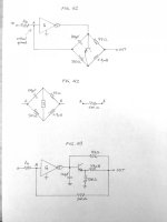
Here's my take on the Quad 405 current dumper. What have I got wrong?
(I'll try not to be too "engineery" but this is an engineering subject after all...😉 )
Fig. Q1 is the same simplified model as Vanderkooy & Lipshitz's except that I have used the actual bridge components and values. I put the real parts in to make it easier to see what is going on.
Here is the crux...
Fig. Q2 shows that the impedance between points A and B of the balanced bridge is 500 ohms. This is independent of any Z in the bridge - shorted, open, transistors, whatever. This is what a balanced bridge does. If it is not balanced then Z plays a role.
In Fig. Q3 I draw an equivalent to Fig. Q1 based on point A being a virtual ground and the bridge connection to point A being replaceable by a single 500 ohm feedback resistor from the output (based on Fig. Q2).
If you have got this far and agree, then please read on.
Fig. Q3 is a conventional NFB circuit around class B (or C if you prefer) power transistors that is relatively easy to understand. It uses the same components as the balanced bridge form but because the feedback is taken directly from the output the circuit is always "balanced" no matter what component values you choose (ie: the Vbe voltages do not have to be balanced out by a bridge because they aren't in the feedback path anymore).
>> So one question I have is why did Quad use the Fig. Q1 circuit rather than the Fig. Q3 circuit as the latter needs no balancing?
Examining Fig. Q3 you can see the 120pF capacitor introduces an integration into the amplifier response. This slows the thing down and helps with the issue Jan pointed out earlier that the voltage on the power transistor bases will tend to slew extremely rapidly. Without the capacitor I image the circuit would be totally unstable.
The 47 ohm resistor allows the amplifier to drive the output directly and this is what happens in the "gap" when both power transistors are off. The open-loop output impedance of the amplifier is about 43 ohms (there is some shunting from the inductor and 500 ohm resistor). This is huge so the NFB is really keeping the output impedance usably low. Note also that the power transistors will start to turn on at around 0.6V, say, so the transconductance amplifier is only supplying about +/-13mA before "dumping" kicks in. Not a lot of class A - pretty much the same as some conventionally biased class AB amps. Note also that since the class A amp has to draw this current all the time there is no net power saving by having unbiased power transistors.
Normally, no designer would put a 2.8uH inductor between their emitter followers and their feedback point. This adds another complex pole in the loop. So I imagine the Quad 405 is a sod to keep stable into difficult loads, especially capacitors.
I wonder whether many of the topology decisions in the Quad stem from trying to stabilize the real circuit.
Bonus question: If you start with the circuit of Fig. Q3, how would you improve it?
Attachments
Last edited:

Not sure. When a BJT turns on it will start to present a decreasing impedance to the transconductance amplifier. The inductor will make this impedance higher at higher f. In this sense, the inductor impedes the speed of current flow through the BJT. The NFB will try to make the output follow the input anyway and force even more current through the BJT & 47 ohm resistor by putting more voltage across them which will also be non-linear.No, if you think about what happens from a qualitive point of view, as the output transistors switch there is step change, as the output transistor is fed into an inductor these high order harmonics see a high impedance load and are attenuated, these then see the class A error correcting amplifier, which being class A is low input impedance attenuating the harmonics further.
I think I get what you mean but I also think there is no free-lunch and the distortion products will be diverted rather than removed. This is a little too qualitative for me...I prefer diagrams and equations. Mind you, reading that Vanderkooy & Lipshitz paper isn't exactly my idea of a good time.
If you don't trust the equations, then qualitive is the only other way!. I did post an Ltspice current dumping amplifier earlier, have a play with it and look at the signals before and after the bridge and with the bridge out of balance.
Correction to post #62
The output Z in the gap at low f will be a lot higher than 43 ohms, closer to 250. This drops as the power transistors turn on. It needs simulation if interested. The key point is that it relies on NFB for usably low output Z.
The output Z in the gap at low f will be a lot higher than 43 ohms, closer to 250. This drops as the power transistors turn on. It needs simulation if interested. The key point is that it relies on NFB for usably low output Z.
Here's my take on the Quad 405 current dumper. What have I got wrong?
(I'll try not to be too "engineery" but this is an engineering subject after all...😉 )
Fig. Q1 is the same simplified model as Vanderkooy & Lipshitz's except that I have used the actual bridge components and values. I put the real parts in to make it easier to see what is going on.
Here is the crux...
Fig. Q2 shows that the impedance between points A and B of the balanced bridge is 500 ohms. This is independent of any Z in the bridge - shorted, open, transistors, whatever. This is what a balanced bridge does. If it is not balanced then Z plays a role.
It is easy to see that this is wrong. Just substitute Z -> infinity (remove Z) and calculate the impedance between A and B at zero frequency and for frequencies approaching infinity:
f = 0: capacitor is an open circuit, inductor a short circuit -> impedance between A and B is 500 ohm.
f -> infinity: capacitor becomes a short circuit, inductor an open circuit -> impedance between A and B is 47 ohm.
In fact you get the same values for the impedance between A and B at zero and at infinite frequency for any value of Z, removing it just simplifies things a bit.
In Fig. Q3 I draw an equivalent to Fig. Q1 based on point A being a virtual ground and the bridge connection to point A being replaceable by a single 500 ohm feedback resistor from the output (based on Fig. Q2).
If you have got this far and agree, then please read on.
I don't. Your Fig. Q2 is wrong and even if it were correct, the step from Q1 to Q3 would be unclear.
The way I see it is as follows. It is an oversimplified analysis that neglects all kinds of second-order effects, but it does explain the basic operation:
Look at Q1 but replace the dumpers with an independent voltage source connected between ground and the node between the 500 ohm resistor and the 2.8 uH inductor. You then have a simple linear time-invariant model. If you can show that the transfer from the independent voltage source to the output is zero, then it doesn't matter what the voltage provided by the voltage source looks like. In particular, it doesn't matter if it is a distorted version of the signal you want to listen to.
Since the model is linear, you might as well calculate the transfer to the short-circuit current from the output, rather than the voltage. When the transfer to the short-circuit current is zero and the output impedance is finite, the transfer to the open-circuit voltage must also be zero.
The voltage Vdumper produces a current Vdumper/(j omega L) through the inductor to the output. That is, the current is inversely proportional to frequency and has a phase shift of -90 degrees.
Voltage Vdumper also produces a current Vdumper/500 ohm into the virtual ground node, assuming a perfect virtual ground. Due to the 120 pF feedback capacitor, the output voltage of the integrating class-A part is -Vdumper/(j omega 500 ohm 120 pF). Through the 47 ohm resistor, this gives an output short-circuit current of -Vdumper/(j omega 500 ohm 120 pF 47 ohm).
The total short-circuit output current due to Vdumper is Vdumper/(j omega) * (1/L - 1/(500 ohm*120 pF*47 ohm)). This expression becomes zero when L = 500 ohm*120 pF*47 ohm = 2.82 uH. The path through the inverting integrator then precisely cancels the path through the inductor.
Back from the model to reality: in reality there is a cancellation, just like in the oversimplified model, but there are some imperfections that limit its efficacy, such as:
-Component tolerances.
-Finite DC gain of the class-A integrating amplifier and nonzero DC resistance of the coil. As it so happens, these compensate each other to some extent.
-Distorted dumper base currents causing error voltages across the nonzero output impedance of the integrator (Lipshitz and Vanderkooy model this with a finite open-loop transconductance of the integrator).
-Bandwidth limitations of the integrator - these can probably be partly compensated for by tweaking the bridge components, which may explain why Quad uses 3 uH instead of 2.82 uH.
By the way, I do agree with your claim that the circuit uses feedback, the integrator is clearly a feedback circuit. Current dumping is a combination of negative feedback and a very clever cancellation scheme.
Last edited:
Hi Marcel!
What do you think, wich amp topology/error correction is the most promissing regarding sq now?
This is just my two cent's worth, but I have the impression that amplifier designers generally spend too much attention to nonlinearities and too little to linear errors, such as roll-off near the band edges. Loudspeaker designers typically do the opposite, worry a lot about linear errors and not about distortion. Of course loudspeakers produce mainly low-order distortion, but still...
That's how I explained how the circuit works to myself. I was inspired by Peter Baxandall's analysis in MichaelTalbot-Smith's Audio Engineer's Reference Book, second edition pages #133-134.Look at Q1 but replace the dumpers with an independent voltage source connected between ground and the node between the 500 ohm resistor and the 2.8 uH inductor. You then have a simple linear time-invariant model. If you can show that the transfer from the independent voltage source to the output is zero, then it doesn't matter what the voltage provided by the voltage source looks like. In particular, it doesn't matter if it is a distorted version of the signal you want to listen to.
I agree. I approximated it to a resistor but the resistance does drop by 3dB by about 2.7MHz. I'll update with an exact representation but I don't think this makes a substantive difference to Fig. Q3 aside from some phase lead compensation at high frequencies. Thank you for pointing this out. 🙂It is easy to see that this is wrong. Just substitute Z -> infinity (remove Z) and calculate the impedance between A and B at zero frequency and for frequencies approaching infinity:
Aside from this, is there anything substantively different between Fig Q1 and Fig Q3?
I'll address your other points soon.
Let's name the upper node "C" and the lower node "D". D is the junction between the inductor and the 500 ohm resistor.The way I see it is as follows. It is an oversimplified analysis that neglects all kinds of second-order effects, but it does explain the basic operation:
Look at Q1 but replace the dumpers with an independent voltage source connected between ground and the node between the 500 ohm resistor and the 2.8 uH inductor. You then have a simple linear time-invariant model. If you can show that the transfer from the independent voltage source to the output is zero, then it doesn't matter what the voltage provided by the voltage source looks like. In particular, it doesn't matter if it is a distorted version of the signal you want to listen to.
You describe attaching a voltage source between D and ground?
If so, the transfer from the voltage source to the output, node B, will definitely not be zero. The bridge function requires both C and D nodes to float. But a voltage change between C and D will not transfer to the output.
Member
Joined 2009
Paid Member
The L & V paper on feedforward amplifiers was for me one of the highlights of reading technical publications about this hobby. A very nicely written paper that I enjoyed going through and reproducing the match with pencil and paper. The issue with this feed forward approach is that it requires the summing of signals at the output (bridge). Because you can't add signals in the voltage domain you end up with an amplifier with negative feedback. Although I haven't tried it, I suggest applying the feedforward scheme to a current mode output amplifier to see if you can engineer a circuit that doesn't require any loop feedback.
The current flowing from node A to the virtual ground will always be [v(B) - v(A)]/Z where Z is the impedance between nodes A and B.I don't. Your Fig. Q2 is wrong and even if it were correct, the step from Q1 to Q3 would be unclear.
Therefore, the connection between virtual ground and A can be replaced with an impedance Z between virtual ground and node B (output) and node A can be grounded.
Virtual ground is assumed to be close enough to ground to make no substantive difference.
Quad listening test and related article links
I found a LTE by Norman Marsh to EW/WW Dec 1982 on the A/B double-blind listening test method which was used by Quad.
Also Keith Snook has the EW/WW Dec 1975 Quad 405 article and the Quad 405 Brochure with specs and John Linsley Hood explained the basic operation of "current dumping" in EW/WW Dec 1989 (Fig 5 on p10 of the PDF). I thought they me be of some interest.
Cheers
There was an article in EW/WW by James Moir on the Quad amp comparisons (Table 1 shows the stats).No, I only have a second-generation paper copy made in the early 1990's. Of course I could scan that copy for you, if you like.
I found a LTE by Norman Marsh to EW/WW Dec 1982 on the A/B double-blind listening test method which was used by Quad.
Also Keith Snook has the EW/WW Dec 1975 Quad 405 article and the Quad 405 Brochure with specs and John Linsley Hood explained the basic operation of "current dumping" in EW/WW Dec 1989 (Fig 5 on p10 of the PDF). I thought they me be of some interest.
Cheers
I agree. I approximated it to a resistor but the resistance does drop by 3dB by about 2.7MHz. I'll update with an exact representation but I don't think this makes a substantive difference to Fig. Q3 aside from some phase lead compensation at high frequencies. Thank you for pointing this out. 🙂
Aside from this, is there anything substantively different between Fig Q1 and Fig Q3?
Yes, Q1 is a very clever distortion cancellation circuit whereas Q3 isn't.
The current flowing from node A to the virtual ground will always be [v(B) - v(A)]/Z where Z is the impedance between nodes A and B.
You completely ignore the fact that there are things connected to the "bridge" at other points than only nodes A and B. If both the output of the class-A amplifier and the dumper were connected at node A or node B, I would agree, but they are not.
Therefore, the connection between virtual ground and A can be replaced with an impedance Z between virtual ground and node B (output) and node A can be grounded.
Hence, this statement is also wrong.
Let's name the upper node "C" and the lower node "D". D is the junction between the inductor and the 500 ohm resistor.
You describe attaching a voltage source between D and ground?
Yes, I do.
If so, the transfer from the voltage source to the output, node B, will definitely not be zero. The bridge function requires both C and D nodes to float. But a voltage change between C and D will not transfer to the output.
If you forget for the moment that there are people who call it a bridge, do you see any flaw in my calculation?
There was an article in EW/WW by James Moir on the Quad amp comparisons (Table 1 shows the stats).
I found a LTE by Norman Marsh to EW/WW Dec 1982 on the A/B double-blind listening test method which was used by Quad.
Also Keith Snook has the EW/WW Dec 1975 Quad 405 article and the Quad 405 Brochure with specs and John Linsley Hood explained the basic operation of "current dumping" in EW/WW Dec 1989 (Fig 5 on p10 of the PDF). I thought they me be of some interest.
Cheers
Hi Ian,
All your links when clicked lead to Keith Snooks' home page. But looking at your post, the URLs are different. What's going on here, is it an issue with Keith's site?
Jan
We shall see.Yes, Q1 is a very clever distortion cancellation circuit whereas Q3 isn't.
I want to use objective analysis to pull back the thick curtain of hyperbole from in front of the current dumping circuit.
Last edited:
- Home
- Amplifiers
- Solid State
- Peter Walker and his current dumping principle