Hi Prasi,
Nice design, I like it.
The recommended heatsink when using a +/- 45Vdc supply is 0.5K/W per channel.
BR,
Eric
Thanks Eric,
Dont have that big heatsink. I will use a smaller Heat sink but with a fan. Also limit the supply voltage to something like 24V for final build if I ever go that far. First need to build second channel and get rid of the hum.
reg
Prasi
Hi guys! 
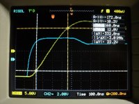
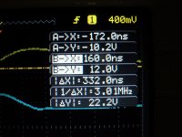
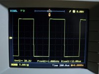
Here is a scope shot of one of my PeeCeeBees amplifying a 140KHz uncleaned square with 60nS rise time. Two 22pF Cdom installed. Input RF shunt and zobel removed.
Happy New Year!!!
(more traces coming)
Here is a scope shot of one of my PeeCeeBees amplifying a 140KHz uncleaned square with 60nS rise time. Two 22pF Cdom installed. Input RF shunt and zobel removed.
Happy New Year!!!
(more traces coming)
Attachments


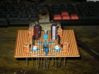
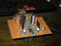
looks a bit like mine, with four channels on strip boards. I'm building two channels of stereo amplification, although I will build a prototype first, to check on CCS and Cdom cap values. I have split the power supplies, so that the output transistors have their own supply, and the Vas its own. I'm wanting to give the input pair their own, too, from a 12 - 15v supply. Total cap count is nearly 100 per stereo channel, with about 10,000uF per rail per amplifier, with much bypassing with poly caps, too.
Pics when I can
Pics when I can
yep, Shaan, I think of an amplifier as a power supply modulator (by the music signal) so the better the p/s, maybe the better the amplifier. 🙂
Splitting the power rails also tends to isolate the saggy output rails from the control signals (Vas and input), IMHO. As the music signal (well, on classical music, which I listen to the most) has only a single transient peak per 'crash', there is time for the power supply to the output transistors to recover, but let the voltage amplifier/s continue to do their own thing, unabated. We will see!
Splitting the power rails also tends to isolate the saggy output rails from the control signals (Vas and input), IMHO. As the music signal (well, on classical music, which I listen to the most) has only a single transient peak per 'crash', there is time for the power supply to the output transistors to recover, but let the voltage amplifier/s continue to do their own thing, unabated. We will see!
I agree. Isolating the rails of everything before power stage has obvious advantages regarding large signal response.
In the meantime...
The new layout is significantly different from the previous PeeCeeBee and the FETs and VAS are targeted to be mounted laterally with the board. Also the feedback caps have been moved to the opposite side of the board. Input is direct coupled.
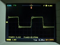
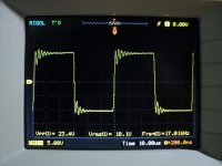
At power-up 40mV offset without setting. Manually set to zero by turning -ve side trimmer. Picture shows 1KHz scope probe calibration output amplified and no sign of ill behavior.
Load tests are next and will be uploaded tomorrow. If successful then layout will be sent to printer for batch printing.
Attachments
hello, i use 246/103 jfet input instead of 550/560. sound good but bias keep climbing until amp unstable. jfets themselves get very warm. how to fix this? thank you.
Hi donovas.
This amp is not designed for using jFETs at input. Instead of jFETs or the original BJTs you can use BC546B/BC556B pair or BC557C/BC547C pair.
All the best.
This amp is not designed for using jFETs at input. Instead of jFETs or the original BJTs you can use BC546B/BC556B pair or BC557C/BC547C pair.
All the best.
A new pcb is on the road!😱The new layout is significantly different from the previous PeeCeeBee and the FETs and VAS are targeted to be mounted laterally with the board. Also the feedback caps have been moved to the opposite side of the board. Input is direct coupled.
At power-up 40mV offset without setting. Manually set to zero by turning -ve side trimmer. Picture shows 1KHz scope probe calibration output amplified and no sign of ill behavior.
Load tests are next and will be uploaded tomorrow. If successful then layout will be sent to printer for batch printing.
Good news😉
Waiting you posting this new pcb!
Regards.
Thimios
thanks shaan. but it works! there must be way to stabilize...
I think so as well, but I don't have experience with jFETs so can't comment. I think you will get help in the pass forum as those people are more used to jFET input amps.
The new layouts are as follow:
1. A mod of the original V1.0 layout with Cdom, better offset control, zobel, corrected silkscreen and direct coupled input. Size - 2" x 2.5". Power approx. 100W into 4R with +/-35V.
2. A mod of the original V2.0 layout with better offset control, Cdom, zobel, lower MOSFET bias and direct coupled input. Size - 4.6" x 2.5". Power approx. 250W into 4R with +/-56V.
3. A fresh compact V3.0 layout with horizontal MOSFET and VAS placement, better offset control, Cdom, zobel and direct coupled input. Size - 2.2" x 2.2". Power approx. 100W into 4R with +/-35V.
The plans are being sent to the fab and will be uploaded as soon as I get the boards at hand. Possibly within first week of Feb.
Need the pdf file for the cap multiplier of MrEvil/PMI used for this amp
This might be it.
Post #507
- Home
- Amplifiers
- Solid State
- PeeCeeBee