Indeed I have everything in the correct place, the trimmers look right, and all GNDs are connected.
I got standart 5mm LEDs in place, should be around 1,8 Votl, got green and red ones.
I suppose the 10k is not mandatory, but helps for accuracy, so I think I wont solder a new resistor in there until it runs at least for a bit of time.
I got standart 5mm LEDs in place, should be around 1,8 Votl, got green and red ones.
I suppose the 10k is not mandatory, but helps for accuracy, so I think I wont solder a new resistor in there until it runs at least for a bit of time.
Attachments
Please connect the SGND to PGND with a small wire or SGND directly to PSU ground with a separate wire.
Re-check the small-signal transistors and the VAS transistors. If all of them are okay then the amp should be running normally. Also check all the resistors if there have been any mistake in placing.
Do you read any oscillation in the output? Does turning VR1 and VR2 have any effect on VAS bias and output offset?
Please connect the SGND to PGND with a small wire or SGND directly to PSU ground with a separate wire.
Re-check the small-signal transistors and the VAS transistors. If all of them are okay then the amp should be running normally. Also check all the resistors if there have been any mistake in placing.
Do you read any oscillation in the output? Does turning VR1 and VR2 have any effect on VAS bias and output offset?
Ok I did the seperate wire to PSU gnd.
gotta recheck the small signal ones, I just to the quick diode testing on them:
No oscillations on the output, I can ajust the output with VR3 ( just realized you did not mean that) anyway, output signal offset can be varies withing roughly 300 mV, but as I turn the VR3 up, the measured current also rises, from 300mA to 450 mA, then I did stop again, since I fear longer on times will hurt some resistors in my PCB, they get quite hot as the high current implies.
VR1 andVR2 dont do anything on the output voltage, I cannot alter anything by turning them, at least it seems so.
Gonna check the Transistors now and will reply soon.
Thanks for your help already.
All transistors read perfectly with the diode test between base collector, base emitter, i did check thrugh all resistors again, couldnt find any anomalies.
Can you say what current you would assume from a frist run, maybe the 350mA on the positive is something one could expect, although the 10R resistor definetly is getting all of that:
so P = I²R, gives over 1 Watt, which will cook the 1/4 rated resistor?!
What would happen if i got the bigmosfet switched, or the medium size bipolar? although the bipolar ist kinda proofed, since i did the diode test on its legs...
Just found a little something, although not critical i mention it before someone else falls about it:
the positions of D3, R21; in the positive, and D4, R22, respectively, seem to be switched in the real PCB!!!
Just for measurment reasons; R21 is the one touching the base of Q3, and D3's anode is connected to the MOSFET base resistor R23!!!
Maybe it wouldnt be too unusefull to make schematic consistent to the PCB 🙂
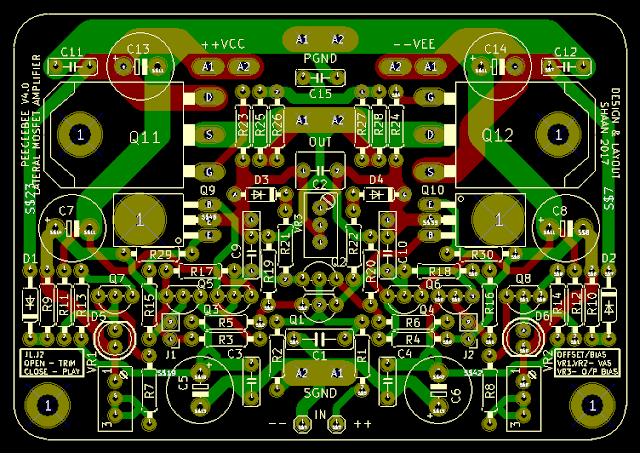
Last edited:
All transistors read perfectly with the diode test between base collector, base emitter, i did check thrugh all resistors again, couldnt find any anomalies.
Can you say what current you would assume from a frist run, maybe the 350mA on the positive is something one could expect, although the 10R resistor definetly is getting all of that:
so P = I²R, gives over 1 Watt, which will cook the 1/4 rated resistor?!
With all default components and with all preliminary steps taken as suggested in the setup guide, VAS current should be as mentioned in the guide, and similar reading should be seen on both R29 and R30. But with less than half of the recommended PSU voltage, you can expect a few things to not work as expected. The two 22K resistor will supply less than half current to both the LEDs and the bases of Q7/Q8, making them running at sub-optimum bias than needed for best CCS stability and balance.
The VAS transistors, if okay and wasn't swapped, is definitely getting more base current than they should. So everything connected to their bases should be checked. I would suggest you remove the board from the heatsink, desolder all transistors and check for any mistake.
What would happen if i got the bigmosfet switched, or the medium size bipolar? although the bipolar ist kinda proofed, since i did the diode test on its legs...
If you switch/swap the MOSFETs then they will pass high current and PSU fuses should be blown. If the PSU have no form of protection then the MOSFETs may blow. Nothing should happen to the previous stages but if internal protection diodes get shorted (2SK/J) due to the fault then expect catastrophe.
Just found a little something, although not critical i mention it before someone else falls about it:
the positions of D3, R21; in the positive, and D4, R22, respectively, seem to be switched in the real PCB!!!
Just for measurment reasons; R21 is the one touching the base of Q3, and D3's anode is connected to the MOSFET base resistor R23!!!
Maybe it wouldnt be too unusefull to make schematic consistent to the PCB 🙂
It doesn't matter in two series placed components if their polarity and designation are correct. It's not critical.
Last edited:
Ok , so first thing, I couldnt really something stating +-15V is not allowed, nor anything about actual recommended input voltages. Now I did follow a link to the firt peeceebee and their you state:
The amp can be run from +/-15V upto +/-35V. The only part that needs to be varied is the default 15K resistors which are for 35V operation. I Use 10K for my 16V setup.
So maybe you could consider posting some more recommended specs on the first page of this thread.
( but I do get this is a diy, so anyone should know what they are doing anyway 🙂 )
So Im checking the VAs bias parts again as you recommended and will solder another 22k in parallel to get the base current up, if I got that right.
So thanks for the ongoing help, I will share in a view what outcome it did bring.
And the last thing...
It does always matter to have board and layout consistent, it becomes critical as soon as troubleshooting begins, and me personally, I never got a board running without troubleshooting 😉
Ok , so first thing, I couldnt really something stating +-15V is not allowed, nor anything about actual recommended input voltages. Now I did follow a link to the firt peeceebee and their you state:
The amp can be run from +/-15V upto +/-35V. The only part that needs to be varied is the default 15K resistors which are for 35V operation. I Use 10K for my 16V setup.
This is V4 and uses CCS. All previous PeeCeeBees didn't. What I said about the voltage remains correct for the previous peeceebees.
I assume the jumper pins are open. The fact that the VAS is passing such high current means that either the two current limiting transistors Q5 and Q6 are not working properly, or C9/C10 is damaged, or there could be other reason that needs to be found.
So maybe you could consider posting some more recommended specs on the first page of this thread.
( but I do get this is a diy, so anyone should know what they are doing anyway 🙂 )
All details related to V4 is in the GB thread. 🙂
The board have been tested many time by myself and others to be free from errors. A few owners of the V4 boards from GB1 have contacted me with reports of malfunction in their setup, and all of them realized that there was either some mistake they were making or didn't follow the guide or overlooked some important points.
So Im checking the VAs bias parts again as you recommended and will solder another 22k in parallel to get the base current up, if I got that right.
So thanks for the ongoing help, I will share in a view what outcome it did bring.

And the last thing...
It does always matter to have board and layout consistent, it becomes critical as soon as troubleshooting begins, and me personally, I never got a board running without troubleshooting 😉
Dont get me wrong, I am convinced I the error is on my side, from the beginning until I got other proof 🙂
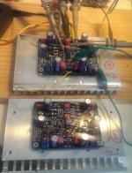
So right now I did manage to at leats produce some magic smoke with one PCB, my supply rails are from a Traco +-15V , but I did connect some 8R2 10W rated in series, so the Peeceebee sees kind of +-11 V, due to the voltage loss, so I thought maybe the whole PCB just hangs up cause of the lack of supply, well I guess I was wrong witht hat thought 🙂
PCB was powered with almost +-15V but after around 20seconds some smoke did appear, so I stopped the measurments , for sure the Q3 did loose its purpose and Q5 also.
I will do some quick checks and replace those.
Ah the death was probably cause, since I did try to play with VR3 to change some offset or at leasts ee anything on the output, then I thought maybe the output signal started oscilating, but I hadnt enough time playing with the scope, adjusting the right timing, before the smoke appeared.
Another strange thing is that the Q9 BD140 is measring 0,694V across collecotr emitter, but I guess that could be some traces around that part, cause I did check another BD140 which isnt soldered in yet and it does not measure such voltages.
Dont get me wrong, I am convinced I the error is on my side, from the beginning until I got other proof 🙂
Sorry I didn't mean to be rude. Poor choice of words on my side.
So right now I did manage to at leats produce some magic smoke with one PCB, my supply rails are from a Traco +-15V , but I did connect some 8R2 10W rated in series, so the Peeceebee sees kind of +-11 V, due to the voltage loss, so I thought maybe the whole PCB just hangs up cause of the lack of supply, well I guess I was wrong witht hat thought 🙂
PCB was powered with almost +-15V but after around 20seconds some smoke did appear, so I stopped the measurments , for sure the Q3 did loose its purpose and Q5 also.
I will do some quick checks and replace those.
Ah the death was probably cause, since I did try to play with VR3 to change some offset or at leasts ee anything on the output, then I thought maybe the output signal started oscilating, but I hadnt enough time playing with the scope, adjusting the right timing, before the smoke appeared.
Another strange thing is that the Q9 BD140 is measring 0,694V across collecotr emitter, but I guess that could be some traces around that part, cause I did check another BD140 which isnt soldered in yet and it does not measure such voltages.
With R3 and R4 (2K2) intact that can only happen through Q3 and Q5's base emitter channel. And a faulty VAS transistor and/or oscillation can make it happen.
The 0.694V across collector and emitter seems to indicate that it's either dead or pushed to some out-of-spec state. Can you check continuity between the VAS transistors' collector pins and the heatsink?
Last edited:
ok. Wow, that did suprise me.
On the broken PCB the VAS BD140 indeed has 1R to the heatsink, both of them do.
On the still working PCB they dont.
I dont see any clue why this could happen, but I think you already know why that is?
What puzzles me is that both PCBs show the same ill not working behaviour, but now that something is broken the VAS Collector is connected to heatsink.
The VCE I assume is due to the resistor diode resistor resisto connection in parallel to my measuring points, if you can follow 🙂 So I assume this is correct.
So another point, the currents are strictly related to voltage and resistors right?
So It has really nothing to do with my less than 15 V supply?
I am close to letting the project go until i find a higher +- power supply, I did work for 6 hours now on getting those damn things to work, and I am loosing a bithope here, I cannot find major flaws on my side of the board.
So the only clue I find is my less voltage supply, which I have seen before some curcuits tend to suck more current when not properly supplied, so maybe if I can organice some plus minus 20V next week I will rewind the issue.
Now that I am thinking,
what would help me would be a map with voltages.
Again my entry point is not 0V, could that be the whole start of the issue, I got DC 1,6V on that point , no matter what I do to the input pin.
The way I see your circuit, there is only one way that VAS is consuming as much current in my place:
disregarding Q5 for a second:
Q3 has to be made conducting, ususally that can only happen, with a (audio) signal applies to the entry. ( Q5 its only purpose is to protect high currents thru Q9, right?)
now what if the constanc current sourced did go nuts?
The forward drop of the standart LED determines the set current right?
With the VR1 to max = 500R + 220R = 720R
the voltage across this, should be lets say 2V for the easiness.
then 2V - VBE = 1,4V ( assume the Vbe drop 0,6V ) this sets the current:
I = 1,94 mA
what is the purpose of the compensation network R13, C5, C3, R5, obviously R19 will provice the feedback path for the current feedback thingie I did read somewhere, but this is always a hard task to grasp on I think for most of us.
so does the constant current of approx 2mA produce 2V on R13 and so on until it hits Q2.
No its complicated, usually I expect a voltage of 0V at the base of the input transistors, what else should it be?
I do measure something else, so maybe there lies the problem in my case.
I am confused, I guess some measurment of other peoples working PCBs would readily help my case a lot. Its always nice to know what to expect.
And in this case the Peeceebee is my first power amp try, and it is a strange kind I must say, I do not find this approach in no book of self nor cordell, or maybe i didnt look sharp enough 🙂
ok. Wow, that did suprise me.
On the broken PCB the VAS BD140 indeed has 1R to the heatsink, both of them do.
On the still working PCB they dont.
I dont see any clue why this could happen, but I think you already know why that is?
What puzzles me is that both PCBs show the same ill not working behaviour, but now that something is broken the VAS Collector is connected to heatsink.
VAS transistors' backs should not be shorted to heatsink. Did you use mica or other insulator between the transistors/MOSFETs and heatsink? If yes then there might be some faults in the insulator and it broke allowing the back of the transistors to touch the heatsink.
The VCE I assume is due to the resistor diode resistor resisto connection in parallel to my measuring points, if you can follow 🙂 So I assume this is correct.
The 4148 diodes are reverse biased relative to the power supply polarities. So you can measure a voltage from collector to emitter (red probe to collector and black to emitter), but the same should not happen by probing emitter to collector if the VAS transistors are okay.
So another point, the currents are strictly related to voltage and resistors right?
So It has really nothing to do with my less than 15 V supply?
The current is not so much related to voltage and resistors in V4 as it did in the previous PeeCeeBees. V4 uses CCS which, although is supposed to provide a constant current, can be made to misbehave if they themselves are not biased properly (through the 22K resistors). For proper operation in an undervoltage setup it naturally needs a value less than 22K to keep the LEDs and transistor bases fed with enough bias current.
I am close to letting the project go until i find a higher +- power supply, I did work for 6 hours now on getting those damn things to work, and I am loosing a bithope here, I cannot find major flaws on my side of the board.
So the only clue I find is my less voltage supply, which I have seen before some curcuits tend to suck more current when not properly supplied, so maybe if I can organice some plus minus 20V next week I will rewind the issue.
If the VAS transistors were touching the heatsink anytime when power was on then this can be the sole reason behind all the distress.
Now that I am thinking,
what would help me would be a map with voltages.
Again my entry point is not 0V, could that be the whole start of the issue, I got DC 1,6V on that point , no matter what I do to the input pin.
The way I see your circuit, there is only one way that VAS is consuming as much current in my place:
disregarding Q5 for a second:
Q3 has to be made conducting, ususally that can only happen, with a (audio) signal applies to the entry. ( Q5 its only purpose is to protect high currents thru Q9, right?)
now what if the constanc current sourced did go nuts?
It is the simplest CCS and is hard for it go nuts, other than by overbiasing on underbiasing it (decreasing or increasing 22K value tooo much).
The forward drop of the standart LED determines the set current right?
With the VR1 to max = 500R + 220R = 720R
the voltage across this, should be lets say 2V for the easiness.
then 2V - VBE = 1,4V ( assume the Vbe drop 0,6V ) this sets the current:
I = 1,94 mA
Correct. Measured across R13 or R14 as 1.94V.
what is the purpose of the compensation network R13, C5, C3, R5, obviously R19 will provice the feedback path for the current feedback thingie I did read somewhere, but this is always a hard task to grasp on I think for most of us.
so does the constant current of approx 2mA produce 2V on R13 and so on until it hits Q2.
Correct. C5/C3 is AC feedback short to ground. R5 sets AC gain by passing AC feedback current through C5/C3, and passes upper CCS's output current coming through R13, to Q2 and biases it so that in turn Q2 can bias Q4 and Q10.
No its complicated, usually I expect a voltage of 0V at the base of the input transistors, what else should it be?
I do measure something else, so maybe there lies the problem in my case.
Right it should be less than 1mV at the bases of input transistors. Are you sure that the PSU's Ground supply is working properly? Does the SMPS directly outputs +15V/0V/-15V?
I am confused, I guess some measurment of other peoples working PCBs would readily help my case a lot. Its always nice to know what to expect. And in this case the Peeceebee is my first power amp try, and it is a strange kind I must say, I do not find this approach in no book of self nor cordell, or maybe i didnt look sharp enough 🙂
It uses a bit of both Self and Cordell and a bit of Slone and a few others' ideas, bits and pieces, put together and tested in fire (sort of 🙂) for a long time.
Awaiting your update with properly insulated BD and MOSFETs. 🙂
Last edited:
Q1 till Q8 are double checked from beginning, and all pnps and npns seem to be in the right places.
Thanks for the long answer, ill try to reply or find the missing errors in the next hours, we will see how this goes.
What still puzzles me, besides the short in the heatsink, which obviously is wrong, and would explain a whole lot.
But I do have 2 PCBs here, and both seem 🙂 of course this is tricky to have the same issue.
But from the beginning I only worked with one PCB since the other one showed somewhat even higher currents on the input, so now I think the higher one of course was the shorted, but still.
Now let me recheck and maybe I find some aha moments in my further troubleshoot.
I think next step will be powering up the peeceebe without any heatsink, for a short time, maybe this erases some of my problems
Last edited:
Holy crap, Shaan, I think I found something 😛
But sadly it is kind of a error on your side 🙂
In the schematic and board, I guess you did switch Q1 and Q2 somewhere int he process.
It does make perfect sense, all uneven and even Qs are PNP and NPN type respectively, but in the circuit diagram you did name the transistors wrong.
And guess who just found out that his input "differential" pair ( as it looks like it to me ) is simply wrong transistors.
I did look at your board picture for a while, and di the manual tracing from Q1 the collector is going to R18 and to its negative supply.
Q2 collector is going to R17 and the positive supply, but in your schematic its simply wrong.
I gotta say, this whole thing could have been avoided if you would have made the effort of putting the board files up, instead of those pictures...
But then again, this is diy and I still appreciate your work, just stating what helps to make things easier.
What really wonders me right now, so many PCBs got sold, like over 100, right?
Did really noone else find out that your Q1 and Q2 are switched, so I have to assume there are 98 builders which simply are naturally more intelligent than I am 😉
cannot wait to resolder and write if this did then finally work.
#update 1
Just to clarify, your indications.pdf is correct, there it states Q1,3,5,7 = 556 ( PNP ) ; Q2,4,6,8 = 546 ( NPN )
Last edited:
Ok, I did switch Q1 and Q2 on both PCBs and for now, no more excessive current drawn, looks pretty good until now.
I will start the biasing procedure now and will get back when I produced my first sounds.
And since im a lazy person I simply ask here, with 15V what kind of output power can I expect? into 4R speakers.
I got some cheap speakers here, rated like 100W, I got no real expirience, its of course mandatory to have bigger speakers than power amp, right? since the speaker will blow otherwise.
Holy crap, Shaan, I think I found something 😛
But sadly it is kind of a error on your side 🙂
In the schematic and board, I guess you did switch Q1 and Q2 somewhere int he process.
It does make perfect sense, all uneven and even Qs are PNP and NPN type respectively, but in the circuit diagram you did name the transistors wrong.
And guess who just found out that his input "differential" pair ( as it looks like it to me ) is simply wrong transistors.
I did look at your board picture for a while, and di the manual tracing from Q1 the collector is going to R18 and to its negative supply.
Q2 collector is going to R17 and the positive supply, but in your schematic its simply wrong.
I gotta say, this whole thing could have been avoided if you would have made the effort of putting the board files up, instead of those pictures...
But then again, this is diy and I still appreciate your work, just stating what helps to make things easier.
What really wonders me right now, so many PCBs got sold, like over 100, right? Did really noone else find out that your Q1 and Q2 are switched, so I have to assume there are 98 builders which simply are naturally more intelligent than I am 😉
cannot wait to resolder and write if this did then finally work.
#update 1
Just to clarify, your indications.pdf is correct, there it states Q1,3,5,7 = 556 ( PNP ) ; Q2,4,6,8 = 546 ( NPN )
Indeed! Q1 and Q2 designation have been swapped in the schematic. My apologies. Things would not have been this bad for you if that blunder didn't happen in the schematic which you've been following all this time. Great job finding out the mistake. Congrats and thank you.
That said, more than once I have uploaded and refined the setup guide which has correct indication and the final corrected guide has been linked in the "Important Links" sections of the first post (right above the schematic). The marking is bold for a reason, they are important. I have more than once made the suggestion to follow the guide for placing the components. Wish you could follow that instead. You've admitted that this amplifier is a little unusual in design. If that is the case then I think you should have strictly followed the guide. Or at least could have let me know earlier that you are not following it, or may be in the very least ask me which one to follow or where to start, and you would have been spared of a lot of typing and wasted time.
Ok, I did switch Q1 and Q2 on both PCBs and for now, no more excessive current drawn, looks pretty good until now.
I will start the biasing procedure now and will get back when I produced my first sounds.
And since im a lazy person I simply ask here, with 15V what kind of output power can I expect? into 4R speakers.
I got some cheap speakers here, rated like 100W, I got no real expirience, its of course mandatory to have bigger speakers than power amp, right? since the speaker will blow otherwise.
I'm glad to know its working. Kudos to you for figuring it out yourself. Expect 10-12 watt into 4R.
Indeed! Q1 and Q2 designation have been swapped in the schematic. My apologies. Things would not have been this bad for you if that blunder didn't happen in the schematic which you've been following all this time. Great job finding out the mistake. Congrats and thank you.
That said, more than once I have uploaded and refined the setup guide which has correct indication and the final corrected guide has been linked in the "Important Links" sections of the first post (right above the schematic). The marking is bold for a reason, they are important. I have more than once made the suggestion to follow the guide for placing the components. Wish you could follow that instead. You've admitted that this amplifier is a little unusual in design. If that is the case then I think you should have strictly followed the guide. Or at least could have let me know earlier that you are not following it, or may be in the very least ask me which one to follow or where to start, and you would have been spared of a lot of typing and wasted time.
I'm glad to know its working. Kudos to you for figuring it out yourself. Expect 10-12 watt into 4R.
Just a heads up, the first post of this thread does not contain any information about v4 at all, at leas tI cannot find any.
And in the groupbuy thread, there is some information, but honestly, since there are only 3 documents... most of us will rather rely on schematic and board, which usually is sufficient,sometimes a bom helps, and your assembly insctructions are indeed very good.
If you really wanna document some stuff, then put a consistens board and schematic in those important information, and not a not consistens schematic at the end of the important links section, this does not make sense in any world 😛
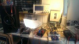
im too lazy right now, but i got some scope shots and measurments ready maybe upload tomorrow.
Thats it for now, call it a day, thanks a lot for the day support shaan, glad that i could test some sounds at last, feels good.
cheers
Just a heads up, the first post of this thread does not contain any information about v4 at all, at leas tI cannot find any.
And in the groupbuy thread, there is some information, but honestly, since there are only 3 documents... most of us will rather rely on schematic and board, which usually is sufficient,sometimes a bom helps, and your assembly insctructions are indeed very good.
If you really wanna document some stuff, then put a consistens board and schematic in those important information, and not a not consistens schematic at the end of the important links section, this does not make sense in any world 😛
Noted.

im too lazy right now, but i got some scope shots and measurments ready maybe upload tomorrow.
Thats it for now, call it a day, thanks a lot for the day support shaan, glad that i could test some sounds at last, feels good.
cheers
My pleasure. I am always available for anything and everything in and around PeeCeeBee. 🙂
- Home
- Amplifiers
- Solid State
- PeeCeeBee