I'm not sure which circuit you are thinking of here. The triple emitter follower ones or the complementary feedback ones.
With the former ones the supply rails connect to the collectors - the voltage on both should stay constant. The supply rails should have local capacitor de-coupling to earth.
With the former ones the supply rails connect to the collectors - the voltage on both should stay constant. The supply rails should have local capacitor de-coupling to earth.
Thank you!
When using a 100...200 watts power transistor the supply voltage is usually high, at least 40V dc ...so it makes senss to give the COB at higher voltages for power transistors.You may argue that the max slew rate of a sine signal is found around crossover where VCB is maximum and a low COB around crossover is more significant than when the emitters approach the rails and the slew rate is minimum.
No. What makes sense is showing a full characterization of Cob x Vcb.
I don't think the choice of vcb=80V is some kind of insight like you suggest. I looked at the full datasheet for the part: https://www.semicon.sanken-ele.co.jp/sk_content/2sc2837_ds_en.pdf
There is no curve of cob x vcb. I'm sure they have the capability to do the test and document this aspect of the part, so if they wanted to give you excellent data they would. More often then not manufacturers choose NOT to show everything.
Last edited:
What do you think , are these distortions (measured on AP) easily achieved in an amp with 120/us slew rate? At the moment when they made the measurements 30 years of use for that amp have passed. That amp was using 2sc2837, two of them in parallel...There's even an amp that has lower thd on 2 ohms using same transistors just lower power in 8 ohms.
Attachments
This looks like a very nice winter amp indeed. Thanks adason for the idea. It's cold down here, very cold in my room now, this amp can work. (BTW I do have very good heating options if I want to. Not using them much now, just taking good care, exercising, keeping warm 🙂)
I'd go for a classic triple with TO92-MOD, TO220 and TO3P. Adason, I think you need to run your drivers hotter, I have 28mA with the single 68 ohm resistor and 700mA bias at the output. 20 volt supplies. Only simulated for the time being.
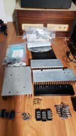
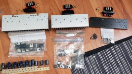
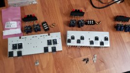
I am in the process of gathering the parts. I got 6 reasonably sized heatsinks. I am waiting for some more mica insulators and resistors.
Sure, I can lower the resistors in the driver. That 200 was just a wild guess.
As long as you are not approaching to slew rate limit of the DUT, there is absolutely no correlation between slew rate and THD/IMD. You may have 1000V/us slewing amp with 1kHz THD of 0.1%, and you may have 15V/us slewing amp with 1kHz and even 10kHz THD of 0.0001%, and vice versa. No correlation. Slew rate just must be several times higher than the highest dv/dt of the useful signal, regarding voltage output. Again, tons of prejudice in audio community.What do you think , are these distortions (measured on AP) easily achieved in an amp with 120/us slew rate?
This design will be used for a prototype. I copied input from PMA’s design as it solves problem of DC anchor point and still serves as bias spreader. Resistors R12 & R13 were removed as they are increasing circuit distortion and serve only as additional unnecessary precaution against possible Siziklai pair oscillation. With that change, calculated distortion drops to 0.0003 @ 1W and remains 0.0015 at almost full power (output peak 3V below rails). At low power levels, distortion profile is even harmonics at +10 dB above odd. Frequency response is up to 10 MHz.

Missing parts for a test build were ordered yesterday and are arriving tomorrow. TME service across EU is really excellent.
LTSpice distortion calculations are usually not very far from the real circuit results, so we’ll see if circuit holds the promise or ends as flop.
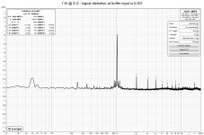
It will be hard to measure with hobby equipment as Focusrite loopback distortion is 0.0003% for small signal levels.
Missing parts for a test build were ordered yesterday and are arriving tomorrow. TME service across EU is really excellent.
LTSpice distortion calculations are usually not very far from the real circuit results, so we’ll see if circuit holds the promise or ends as flop.
It will be hard to measure with hobby equipment as Focusrite loopback distortion is 0.0003% for small signal levels.
Looking forward your measured results. I would bet that your Focusrite will be good enough to measure large signal distortion, in case you have an appropriate voltage divider to reduce amplifier output signal to the card distortion "sweet spot" input level.This design will be used for a prototype. I copied input from PMA’s design as it solves problem of DC anchor point and still serves as bias spreader. Resistors R12 & R13 were removed as they are increasing circuit distortion and serve only as additional unnecessary precaution against possible Siziklai pair oscillation. With that change, calculated distortion drops to 0.0003 @ 1W and remains 0.0015 at almost full power (output peak 3V below rails). At low power levels, distortion profile is even harmonics at +10 dB above odd. Frequency response is up to 10 MHz.
LTSpice distortion calculations are usually not very far from the real circuit results, so we’ll see if circuit holds the promise or ends as flop.
It will be hard to measure with hobby equipment as Focusrite loopback distortion is 0.0003% for small signal levels.
Yes, I count only measured results as well. LTSpice is for help and fun.Looking forward your measured results.
I have all necessary equipment and lowest distortion I managed to measure was 0.0001% for composite input buffer, but at 0.4 V Focusrite’s output. Problem with large signal area is that Focusrite signal generator distortion also rises considerably with rising output level and my standalone signal generator also has varying distortion.
Bet accepted. We'll see. 🙂
I am in the process of gathering the parts. I got 6 reasonably sized heatsinks. I am waiting for some more mica insulators and resistors.
Sure, I can lower the resistors in the driver. That 200 was just a wild guess.
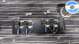
With 100K multi-turn trimpots (below) it should give you a good range of adjustment, even with hot heatsinks. Notice the decoupling for the servo opamp (opa604 can use up to +-24V). I would do this: disconnect servo (open jumper), adjust idle current and dc offset, power down, re-connect servo, measure offset.
Attachments

I've got some parts on the way myself. BTW, onkyo receivers are a great source for toshiba drivers and outputs (sometimes sanken). With all the counterfeiting that's going on, I think onkyo boards and scraps are worth the price. Let's see what the included heatsink can handle.I am in the process of gathering the parts.
If you buy from digikey, you might want to try these:
https://www.digikey.com/en/products/detail/aavid-thermal-division-of-boyd-corporation/4180G/1625664
https://www.digikey.com/en/products/detail/aavid-thermal-division-of-boyd-corporation/4180G/1625664
Silicone thermal pads, capton pads. Why would you use mica???Now that i know mica is mined by children, i am not sure if i want to build too many buffers.
Still gathering heatsinks and parts.
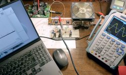
Well, this buffer holds some promise
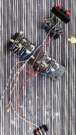
Actual test build is close to component values determined by simulation. Only change is that with 470 pF film capacitors, it was oscillating at 10 MHz with 0.1 V amplitude. Nearest ceramic capacitor at hand was 1 nF, so that was used.
Buffer gain is 0.99 or -0.09 dB.
Bias varies a little and DC offset is very stable. Offset varies just a few mV.
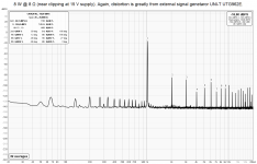
Measured damping factor is 110 at 8Ω. Simply great.
Buffer gain is 0.99 or -0.09 dB.
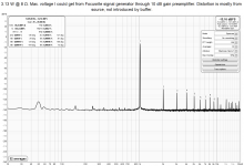
Distortion is very low and tricky to measure with equipment I have as Focusrite’s generator produces signal with increased distortion as output levels rises.
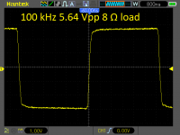
Frequency response of this suboptimal build, based on square wave rise time, is above 1 MHz. Result is affected by test build using low quality high inductance wire wound resistors for R3 & R4, and load is such type as well. That prevents proper power bandwidth measurement.
Now I must kludge together another channel and do some listening.
Actual test build is close to component values determined by simulation. Only change is that with 470 pF film capacitors, it was oscillating at 10 MHz with 0.1 V amplitude. Nearest ceramic capacitor at hand was 1 nF, so that was used.
Buffer gain is 0.99 or -0.09 dB.
Bias varies a little and DC offset is very stable. Offset varies just a few mV.
Measured damping factor is 110 at 8Ω. Simply great.
Buffer gain is 0.99 or -0.09 dB.
Distortion is very low and tricky to measure with equipment I have as Focusrite’s generator produces signal with increased distortion as output levels rises.
Frequency response of this suboptimal build, based on square wave rise time, is above 1 MHz. Result is affected by test build using low quality high inductance wire wound resistors for R3 & R4, and load is such type as well. That prevents proper power bandwidth measurement.
Now I must kludge together another channel and do some listening.
Attachments

My choice are silicone pads for low thermal load and alumina ceramic pads or keratherm for the rest. Never mica.Now that i know mica is mined by children, i am not sure if i want to build too many buffers.
Still gathering heatsinks and parts.
Gents, i was half joking about mica referring to other post. I use mica because it works.
Everytime i use keratherm, which i have plenty, i regret it.
Everytime i use keratherm, which i have plenty, i regret it.
Good job! Those Ccb capacitors (470pF or your 1nF, this depends on output devices speed) are mandatory, in the real circuit.Well, this buffer holds some promise
Actual test build is close to component values determined by simulation. Only change is that with 470 pF film capacitors, it was oscillating at 10 MHz with 0.1 V amplitude. Nearest ceramic capacitor at hand was 1 nF, so that was used.
Buffer gain is 0.99 or -0.09 dB.
Bias varies a little and DC offset is very stable. Offset varies just a few mV.
Measured damping factor is 110 at 8Ω. Simply great.
Buffer gain is 0.99 or -0.09 dB.
Distortion is very low and tricky to measure with equipment I have as Focusrite’s generator produces signal with increased distortion as output levels rises.
Frequency response of this suboptimal build, based on square wave rise time, is above 1 MHz. Result is affected by test build using low quality high inductance wire wound resistors for R3 & R4, and load is such type as well. That prevents proper power bandwidth measurement.
- Home
- Amplifiers
- Solid State
- Output BJTs for buffer