I'm sure it's an excellent device, low cob and all. But Sanken could be more honest by stating the cob at the usual 10V, not 80V.About low cob...
This looks like a very nice winter amp indeed. Thanks adason for the idea. It's cold down here, very cold in my room now, this amp can work. (BTW I do have very good heating options if I want to. Not using them much now, just taking good care, exercising, keeping warm 🙂)
I'd go for a classic triple with TO92-MOD, TO220 and TO3P. Adason, I think you need to run your drivers hotter, I have 28mA with the single 68 ohm resistor and 700mA bias at the output. 20 volt supplies. Only simulated for the time being.
I'd go for a classic triple with TO92-MOD, TO220 and TO3P. Adason, I think you need to run your drivers hotter, I have 28mA with the single 68 ohm resistor and 700mA bias at the output. 20 volt supplies. Only simulated for the time being.
Attachments
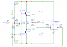

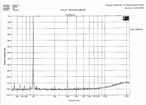
I’m in design evaluation phase and this design is candidate for an actual test build. It can work from +- 10V to -+ 30V. With 1A Iq and +- 15V supply, it will provide up to 8W/8 Ω @ 0.015 % distortion, never leaving pure A class operation. At 1W, distortion is 0.003 %. Harmonic profile is always H2 dominant. Frequency response is up to 6 MHz.

As for the proposed MJL21193/MJL21194, they produce 4x distortion compared to MJL1302/MJL3281 at the same conditions.
As for the proposed MJL21193/MJL21194, they produce 4x distortion compared to MJL1302/MJL3281 at the same conditions.
Attachments
All very good info, keep it comming. Thanks.
I just receiver four heatsinks.
Will build more buffers. Huray.
I just receiver four heatsinks.
Will build more buffers. Huray.
I have nothing against 21193/21194, i just do not have these bjts.
My question was about linearity of those i have.
1302/3281 were highly recommended few times.
My question was about linearity of those i have.
1302/3281 were highly recommended few times.
I have neither. If we are to believe LTSpice simulation with accurate Bob Cordell models for all BJTs, 21193/21194 are producing much more distortion. For circuit with NFB, it could be different.I have nothing against 21193/21194
Can you prove that the FT is better if specified at 10V than at 80 V? By the way, one datasheet specify its cob ac VCB=10V.I'm sure it's an excellent device, low cob and all. But Sanken could be more honest by stating the cob at the usual 10V, not 80V.
That is nice enough however there are nfb loops around Q3/Q4 and Q1/Q2 which need Miller capacitors C4 and C5 for stability which reduce the frequency response.I’m in design evaluation phase and this design is candidate for an actual test build. It can work from +- 10V to -+ 30V. With 1A Iq and +- 15V supply, it will provide up to 8W/8 Ω @ 0.015 % distortion, never leaving pure A class operation. At 1W, distortion is 0.003 %. Harmonic profile is always H2 dominant. Frequency response is up to 6 MHz.
View attachment 1056815
As for the proposed MJL21193/MJL21194, they produce 4x distortion compared to MJL1302/MJL3281 at the same conditions.
I mentioned these transistors because for the meantime they can be bought over the counter here and probably in other parts of the world.
In the proposed circuit the latter have fT figures much lower than BD139 and BD140 so the pole frequency of Q3/Q4 and Q1/Q2 would be due to the the power devices to the point where C4 and C5 could be omitted. In that case their frequency response then could be much the same as quoted for MJL1302/MJL3281.
The simulation takes no account of the increase in temperature above 25 C degrees of running a current of 1A will cause an increase in hFE. The values of resistors are not to suit biasing MJL21193/MJL21194 which have lower hFE anyway and need a little more base current drive current.
hFE (Beta) is not a good yardstick of what the increase may be. There is not much difference if emitter current gain (Alpha) is used instead of base current gain (Beta). Looking at respective datasheets for hFE Alpha would = Beta/(Beta +1) for each.
The result is always less than 1 but the percentage of that is not significantly lower. The gap is lower than many would think.
C4 & C5 are there for compensation on capacitive loads and Siziklai pair stability. There is no gain peaking with capacitive loads up to 10 nF and a very small with 100 nF. They reduce frequency response, but I don’t see an advantage in having more than predicted -3 dB at 6 MHz.
From my perusal of datasheets I learned that Cob is lower at high voltages. Most datasheets state the value of Cob at 10V, like you said, and this makes comparison easy. Best would be a curve of Cob versus voltage of course.Can you prove that the FT is better if specified at 10V than at 80 V? By the way, one datasheet specify its cob ac VCB=10V.
So you're just upset on the manufacturer's choice of specifying the FT for some of their transistors at higher VCB voltages, but your only source of knowledge is just a statistical spread of a factor over more datasheets.I was curious to know why it happens not how it happens.From my perusal of datasheets I learned that Cob is lower at high voltages. Most datasheets state the value of Cob at 10V, like you said, and this makes comparison easy. Best would be a curve of Cob versus voltage of course.
I'm not upset.
It's not the ft, it's the cob that was stated at an unusually high voltage. Manufacturers do this sort of thing on datasheets to make the parts look good. It's a bit misleading. Many people will look at the low cob figure, much lower than what they saw in other datasheets, without realizing that it's only true at high voltage.
It's not the ft, it's the cob that was stated at an unusually high voltage. Manufacturers do this sort of thing on datasheets to make the parts look good. It's a bit misleading. Many people will look at the low cob figure, much lower than what they saw in other datasheets, without realizing that it's only true at high voltage.
First, you will need to define input DC for Q7/Q8, otherwise the output DC will be floating according to NPN-PNP non-symmetry and temperature. Simulation will probably not show it, and also the 4x times distortion reduction with 1302/3281 is not achievable in a real circuit. Re stability, 21193/4 are easier to work with.I’m in design evaluation phase and this design is candidate for an actual test build. It can work from +- 10V to -+ 30V. With 1A Iq and +- 15V supply, it will provide up to 8W/8 Ω @ 0.015 % distortion, never leaving pure A class operation. At 1W, distortion is 0.003 %. Harmonic profile is always H2 dominant. Frequency response is up to 6 MHz.
View attachment 1056815
As for the proposed MJL21193/MJL21194, they produce 4x distortion compared to MJL1302/MJL3281 at the same conditions.
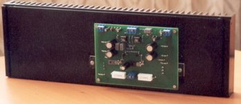
I built (built, not only simulated) a similar class A amp 20 years ago.
Attachments

Yes, I know. This is just feasibility checkup, not exact circuit to build. If breadboard version will deliver good results, proper build will likely use DC servo. I had some fun with inverting version here.First, you will need to define input DC for Q7/Q8, otherwise the output DC will be floating according to NPN-PNP non-symmetry and temperature.
I built (built, not only simulated) a similar class A amp 20 years ago.
You’ve probably built more than most members merely simulated. 🙂
This design is a very good addition to this thread. Thanks.
You might like to split R9 (260 ohm) into two 130 ohm resistors and put the R1R2 common point just there. It should have same parameters + DC stability.Yes, I know. This is just feasibility checkup, not exact circuit to build. If breadboard version will deliver good results, proper build will likely use DC servo. I had some fun with inverting version here.
I have checked this option as well because it makes DC coupled amplifier. However, it was put aside as bias setting is very inconvenient and affects DC offset at the same time. For a fixed Iq value it would be OK and I might end with that solution.You might like to split R9 (260 ohm) into two 130 ohm resistors and put the R1R2 common point just there. It should have same parameters + DC stability.
That is due to the fact that the voltage applied at the collector determines the width of the diffusion and the relationship is an inverse one. Considering the area of the silicon slice and not the depth, this width is more or less in inverse proportion to the square root of the applied collector voltage.I asked you a bit of information: please tell me why is that at high VCB the cob is lower!
In a common emitter stage the collector load causes the collector voltage to vary. This gives rise to Early Effect also known as base-width modulation. When this base width expands there is not as much amplification as one might expect.
Early Effect was described by E.Wolfendale in 1963 in his book entitled "The Transistor An Introduction to Its Applications". I have a copy of this but you could study this on the internet.
While one can look at datasheets for cob information, for simulation purposes one can also look at Cordell's .model sheet or those from other sources.
The parameter to check is CJC meaning base-collector zero- bias p-n capacitance which is stated in Farads.
For example BD139 according to Cordell has 49e-12 meaning 49pF while BD140 has 68e-12 meaning 68 pF.
Early Effect was described by E.Wolfendale in 1963 in his book entitled "The Transistor An Introduction to Its Applications". I have a copy of this but you could study this on the internet.
Thanks for the book recommendation
Thank you!That is due to the fact that the voltage applied at the collector determines the width of the diffusion and the relationship is an inverse one. Considering the area of the silicon slice and not the depth, this width is more or less in inverse proportion to the square root of the applied collector voltage.
In a common emitter stage the collector load causes the collector voltage to vary. This gives rise to Early Effect also known as base-width modulation. When this base width expands there is not as much amplification as one might expect.
Early Effect was described by E.Wolfendale in 1963 in his book entitled "The Transistor An Introduction to Its Applications". I have a copy of this but you could study this on the internet.
While one can look at datasheets for cob information, for simulation purposes one can also look at Cordell's .model sheet or those from other sources.
The parameter to check is CJC meaning base-collector zero- bias p-n capacitance which is stated in Farads.
For example BD139 according to Cordell has 49e-12 meaning 49pF while BD140 has 68e-12 meaning 68 pF.
When using a 100...200 watts power transistor the supply voltage is usually high, at least 40V dc ...so it makes senss to give the COB at higher voltages for power transistors.You may argue that the max slew rate of a sine signal is found around crossover where VCB is maximum and a low COB around crossover is more significant than when the emitters approach the rails and the slew rate is minimum.
- Home
- Amplifiers
- Solid State
- Output BJTs for buffer