Yes, but don't we want to make the output faster?
I am playing with your asc file AndriyOL but God Knows I don't know how to interpret the results 😀
Lots of fun anyway...curves are running parallel beyond 10MHz. 😕
How to make the classical 1KHz sine to evaluate power output and clipping?
Thanks.
M.
I am playing with your asc file AndriyOL but God Knows I don't know how to interpret the results 😀
Lots of fun anyway...curves are running parallel beyond 10MHz. 😕
How to make the classical 1KHz sine to evaluate power output and clipping?
Thanks.
M.
Last edited:
Lots of fun anyway...curves are running parallel beyond 10MHz. 😕
Thanks.
M.
Meaning they do not cross each other...
It's in a properties of source input. Please take a look maybe 20 pages back where Mjona explained in details how to use Spice.
I suppose you applied cascoded output in the schematic.
Please share it here and someone more familiar with Spice will interpret it.
Cheers.
I suppose you applied cascoded output in the schematic.
Please share it here and someone more familiar with Spice will interpret it.
What do you mean by regular one?I have an all BJT-VSSA, with cascaded/cascoded outputs running for months on the patio system, so far stable (39pF CDom; no zobel) and better sounding IMHO than the regular one.
Cheers.
Last edited:
A change of tack
I have been looking for proof that the "balanced" version of this circuit does not work full stop with both signal inputs in phase.
If this set up could be made stable then a separate stage would be needed to process balanced lines and feed the combined output into both inputs of the present circuit.
To demonstrate my point I started looking through my old simulations to find one suitable to use and with a view to cleaning out a lot of older ones.
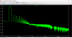
Quite a few of these got close and the thought occurred a Thiele stability network instead of the usual zobel might do the trick and the Bode plots looked satisfactory. This all came unwound when I simulated the circuit for THD at 1 kHz when the plot was totally fuzzed.
Going through these simulations one by one I came across one that was different. This one is stable and it doesn't output fuzz at 1kHz however the THD% is a rather modest 0.038 which I think would be improved with some refinements.
I have been looking for proof that the "balanced" version of this circuit does not work full stop with both signal inputs in phase.
If this set up could be made stable then a separate stage would be needed to process balanced lines and feed the combined output into both inputs of the present circuit.
To demonstrate my point I started looking through my old simulations to find one suitable to use and with a view to cleaning out a lot of older ones.
Quite a few of these got close and the thought occurred a Thiele stability network instead of the usual zobel might do the trick and the Bode plots looked satisfactory. This all came unwound when I simulated the circuit for THD at 1 kHz when the plot was totally fuzzed.
Going through these simulations one by one I came across one that was different. This one is stable and it doesn't output fuzz at 1kHz however the THD% is a rather modest 0.038 which I think would be improved with some refinements.
Attachments
The distortion is the proof that it doesn't work. Otherwise you must consider the distortion a feature. Who knows, maybe it will sound fine? But if you are comparing it to the amps it resembles, then the THD figure should indicate something has gone wrong.
The second input pair is shunting the feedback to ground resistor. Now all of the feedback current (which is a lot since this is a CFA) must be handled by the second input pair. It can't do his linearly. One proper solution would be to replace it with a very good buffer, an opamp would commonly be used like this.
Imagine a simple LTP amp. Add a 3rd transistor to the LTP and try to use it as a negative input. What happens? This is not exactly analogous to what was done here but it is the same kind of logical error.
Last edited:
Proof.
Attached is a simplified input stage and VAS that shows visible distortion when the second input stage is added with all jumpers closed.


BTW Jumpers X5 and X6 are to remove C23 and C26 because they were not in the original Lazy Cat circuit I found here
Simple Symetrical Amplifier
Nevertheless, removing these capacitors still does not seem to make the added input stage work as a differential input.
Unless someone can make the Lazy Cat "balanced" stage operate with low distortion as a differential input stage then as keantoken asserts the input stage does not work as suggested by Lazy Cat in the post above.
I have been looking for proof that the "balanced" version of this circuit does not work full stop with both signal inputs in phase.
Attached is a simplified input stage and VAS that shows visible distortion when the second input stage is added with all jumpers closed.
BTW Jumpers X5 and X6 are to remove C23 and C26 because they were not in the original Lazy Cat circuit I found here
Simple Symetrical Amplifier
Nevertheless, removing these capacitors still does not seem to make the added input stage work as a differential input.
Unless someone can make the Lazy Cat "balanced" stage operate with low distortion as a differential input stage then as keantoken asserts the input stage does not work as suggested by Lazy Cat in the post above.
Attachments
Last edited:
It's in a properties of source input. Please take a look maybe 20 pages back where Mjona explained in details how to use Spice.
I suppose you applied cascoded output in the schematic.
Please share it here and someone more familiar with Spice will interpret it.
What do you mean by regular one?
Cheers.
By regular I mean non-cascoded, both Mosfet and BJT output.
Dear AndriyOL, I would post my 30 minutes effort only if you promise not to laugh 😀 and bear in mind that:
a) These are the kind of crazy experiments that I love to do.
b) I don't know what I am talking about.
Briefly, I made a kind of inverted Common emitter cascode (I did not have the time to think about proper biasing) for the outputs, I cascoded the drivers and integrated them to the feed-back, added degeneration here and there, there are infinite combinations possible and this is the fun of it. I wish I knew how to use spice before... I could not evaluate distortion nor clipping behavior.
Anyway, as I commented before in the AMNESIS thread and others, to me the cascaded or cascoded outputs simply sound more like music, so I am modifying all my outputs.
Best wishes and be nice as I am in my sensitive days...
M.
Attachments
Why not add one more Q14, Q15 to make diff VAS? Connect Q12, Q13 collectors to their bases.Attached is a simplified input stage and VAS that shows visible distortion when the second input stage is added with all jumpers closed.
Problems arise when someone adopts a design intended for high power running from 60 volt supply rails (yours) and reduces those to 45 volts.
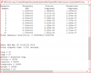
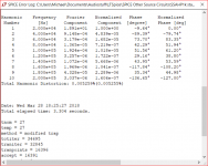
If one re-scales two resistor values - R10 and R11 the 1kHz THD reduces to 0.006%.
When that is done the front end currents look a lot better.
The Vbe bias adjustment is compromised by the reduction in the supply rail voltage. To me and probably others too, it would be better that any changes in scheme be your work rather than mine.
My .asc's need some tidying up of the component numbers but they may be useful to you in this unfinished form.
Dear AndriyOL, I would post my 30 minutes effort only if you promise not to laugh 😀 and bear in mind that:
a) These are the kind of crazy experiments that I love to do.
b) I don't know what I am talking about.
Don't worry, our goal here is not to laugh but solve technical issues. Do not hesitate to take a part.
Cheers.
Do you want to say that the circuit is working as intended with higher rail voltages?Problems arise when someone adopts a design intended for high power running from 60 volt supply rails (yours) and reduces those to 45 volts.
My .asc's need some tidying up of the component numbers but they may be useful to you in this unfinished form.
Last edited:
Why not add one more Q14, Q15 to make diff VAS? Connect Q12, Q13 collectors to their bases.
Can you show what you mean? Do you use LTspice. Mod my circuit.
I tried 2 variants (attached). But none of these gave differential input with low distortion.
- - -
An OOPs😱
There is a fault in my previous simplified circuit. The bases of Q12,Q13 should not be grounded. My apology. Also the sign gen inverter (E2) was +1 when it should be -1.
I've attach the corrected version. Edit: token expired so I'll put attachments in another post
With these fixed the distortion issue is not fixed. There is still a fundamental flaw with the added stage. If you drive the second input with the same phase as the first input the distortion is 10 times higher than with no second input tr's (links open)!
So in it's original form (ie without C23 C26) the additional "differential" parts serve no helpful purpose -- they don't give a differential input and they give higher distortion.
The best idea to get a balanced amplifier so far using this circuit, without any opamps, seems to be the bridge -- two of these amps per channel, each with SE inputs.
Last edited:
missing attachments
token expired so I'll put attachments in another post
Attachments
More Simulations
The first four simulations are self explanatory - the last one is not.
What that showed was a happy state of affairs in the quasi LTP sets (they both looked the same).
The output stage was not working properly then and when I got it to do that and checked my work I found the spikes had returned.
The first four simulations are self explanatory - the last one is not.
What that showed was a happy state of affairs in the quasi LTP sets (they both looked the same).
The output stage was not working properly then and when I got it to do that and checked my work I found the spikes had returned.
Attachments

Why not add one more Q14, Q15 to make diff VAS? Connect Q12, Q13 collectors to their bases.
I tried to follow LC advice. These are the results I got. Which one is correct?
However input bias current aren't symmetrical.
Thanks.
Attachments
Last edited:
I've revised the schematic correspondingly. Serial and Parallel updated.
Attachments
Last edited:
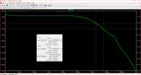
60 Volt rail Simulations.
More attachments.
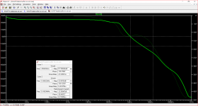
The Bode simulation indicates stability . I added a 2uF cap in parallel with the 8R load. Doing this lifts the gain line and smooths a mild bump in the plot.
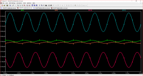
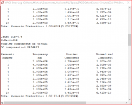
The second image shows THD at 20 khz declines with lowering the signal input level. With the highest test signal level it was 0.008%. I did a multi run of signal level inputs to display the results in a single test.
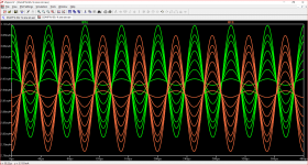
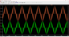
The last two files show the quasi LTP currents the first is the front end one. Again the patterns show multiple signal level input results. Now there are no glitches to be seen.
More attachments.
The Bode simulation indicates stability . I added a 2uF cap in parallel with the 8R load. Doing this lifts the gain line and smooths a mild bump in the plot.
The second image shows THD at 20 khz declines with lowering the signal input level. With the highest test signal level it was 0.008%. I did a multi run of signal level inputs to display the results in a single test.
The last two files show the quasi LTP currents the first is the front end one. Again the patterns show multiple signal level input results. Now there are no glitches to be seen.
Attachments
- Home
- Amplifiers
- Solid State
- One of the Top Solid-State CFA amp design