Now, here's the scope plot that is the crux of all our discussions. To recap, here's what we know:
1) The tempco of the diode is not the same as for the transistor when measured using an isothermic test setup.
2) The temperature of the diode is never the same as that of the transistor's die.
3) The dynamic tempco of the diode/transistor is unknown.
I endeavored to find a If value for the diode to match the dynamic tempcos of the diode and transistors by increasing If in 1 mA increments until they tracked as well as could be attained. Like the datasheet implys, matching should occur at an If of 7 mA. As it turns out, this is true!
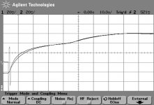
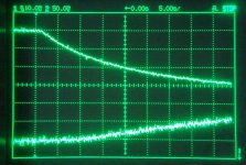
This test shows the tracking between the diode with If=7mA, and the transistor with Ic=100mA (typical standing value).
The transistor is mounted on a heatsink just like in "real life." A curve tracer was used to induce a thermal event to heat the transistor and the heatsink by increasing collector current to 6A for about 30 seconds.
The collector current was returned to 100 mA and the attached scope plot shows Vf of the diode and Vbe of the transistor as the unit cools. They track within 5 mV and the two traces are superimposed for much of the transition!
Bear in mind that this test was using the 4xxx series, not the 3xxx series. I would expect the 3xxx series to yield entirely different data...
Seems to me this answers the questions for the 4xxx's once and for all...
Cheers,
John
1) The tempco of the diode is not the same as for the transistor when measured using an isothermic test setup.
2) The temperature of the diode is never the same as that of the transistor's die.
3) The dynamic tempco of the diode/transistor is unknown.
I endeavored to find a If value for the diode to match the dynamic tempcos of the diode and transistors by increasing If in 1 mA increments until they tracked as well as could be attained. Like the datasheet implys, matching should occur at an If of 7 mA. As it turns out, this is true!
This test shows the tracking between the diode with If=7mA, and the transistor with Ic=100mA (typical standing value).
The transistor is mounted on a heatsink just like in "real life." A curve tracer was used to induce a thermal event to heat the transistor and the heatsink by increasing collector current to 6A for about 30 seconds.
The collector current was returned to 100 mA and the attached scope plot shows Vf of the diode and Vbe of the transistor as the unit cools. They track within 5 mV and the two traces are superimposed for much of the transition!
Bear in mind that this test was using the 4xxx series, not the 3xxx series. I would expect the 3xxx series to yield entirely different data...
Seems to me this answers the questions for the 4xxx's once and for all...
Cheers,
John
Attachments
Re: Re: Re: Re: Crossover distortion and biasing dynamics
Hi JPV,
The concept of the thermal resistive divider extending from the BJT junction to the heatsink, with the diode sitting in the middle of the divider is useful, but there is a key area for potential misunderstanding.
I suspect that your way of looking at it has the voltage divider being driven by a voltage source, whereas my way of looking at it has the divider being driven by a current source.
I believe that the proper electrical analog for the heat source (the BJT junction) is a current source. This makes a big difference.
First, for simplification, we are ignoring heat loss through the plastic case to ambient. Any such heat loss will act as a shunt resistance that will lower the Thevenin impedance of the heat source. If the heat source is a perfect "current" source, all of the heat will flow through the resistors of the resistive divider. Under these conditions, the static temperature difference between the BJT junction and the diode will simply depend on the thermal resistance of the "input" resistor of the thermal resistive divider, which I'm assuming to be about 0.7 C/W. The temperature difference does not depend on the thermal resistance of the insulator or of the heat sink.
A voltage divider fed from a current source does not act as a divider in the way that you are ssuming, I think.
The dynamic action you describe would happen as described if the heat source behaved like a voltage source.
The delta T between BJT junction and diode will be vastly different under the two conditions of high and low dissipation. BTW, it is certainly true that a delta T will exist even under the 100 mA bias condition, but this will be small compared to high-current operating conditions. The power transistor in the example I cited with 100 mA bias and 35V rail dissipates 3.5W at idle, but about 14W at 1/3 power. Thus, we might expect a delta T at idle of about 3.5 X 0.7 = 2.45C, corresponding to perhaps 5 mV or so.
Cheers,
Bob
JPV said:
I still have a problem:
Let suppose that we start from idle. The junction is seeing some bias power dissipated and its temperature is above the one of copper and diode in proportion to the thermal resistance dividers.
The heatsink is at another stable temperature below the others.
Then we apply a step of power. After vanishing of die and solder transients, the die, copper (so the diode) and heatsink will experience the long time constants of copper and heatsink but in the same manner. Although all the temperatures are still drifting, the die and diode temperature remain at proportional temperatures, the coef of proportionnality is set by the thermal resistor dividing action.. The same will happen on cooling after removing of the signal power until we reach the temperatures set by the bias dissipation. The transients of the die will induce mistraking but the transients induced by the copper and heatsink will be applied to both.
If this is correct the tuning of the tempco can compensate for this and the mistracking will happen only during the short time constant of the die. It is the delta T that matters.
Am I wrong ?
JPV
Hi JPV,
The concept of the thermal resistive divider extending from the BJT junction to the heatsink, with the diode sitting in the middle of the divider is useful, but there is a key area for potential misunderstanding.
I suspect that your way of looking at it has the voltage divider being driven by a voltage source, whereas my way of looking at it has the divider being driven by a current source.
I believe that the proper electrical analog for the heat source (the BJT junction) is a current source. This makes a big difference.
First, for simplification, we are ignoring heat loss through the plastic case to ambient. Any such heat loss will act as a shunt resistance that will lower the Thevenin impedance of the heat source. If the heat source is a perfect "current" source, all of the heat will flow through the resistors of the resistive divider. Under these conditions, the static temperature difference between the BJT junction and the diode will simply depend on the thermal resistance of the "input" resistor of the thermal resistive divider, which I'm assuming to be about 0.7 C/W. The temperature difference does not depend on the thermal resistance of the insulator or of the heat sink.
A voltage divider fed from a current source does not act as a divider in the way that you are ssuming, I think.
The dynamic action you describe would happen as described if the heat source behaved like a voltage source.
The delta T between BJT junction and diode will be vastly different under the two conditions of high and low dissipation. BTW, it is certainly true that a delta T will exist even under the 100 mA bias condition, but this will be small compared to high-current operating conditions. The power transistor in the example I cited with 100 mA bias and 35V rail dissipates 3.5W at idle, but about 14W at 1/3 power. Thus, we might expect a delta T at idle of about 3.5 X 0.7 = 2.45C, corresponding to perhaps 5 mV or so.
Cheers,
Bob
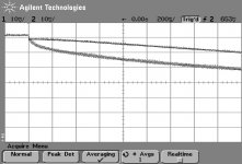
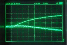
jgedde said:Here's some more data on the NJL4281/4302. The attached scope capture shows the thermal time constant between the diode and the transistor's Vbe.
No attempt was made to match tempcos as the purpose of this test was to measure how fast the diode would respond to temperature changes in the transistor.
This test was performed with two curve tracers. One was supplying the compensation diode with a 10 mA constant current. The other tracer was driving the transistor. The transistor was ounted on a heatsink.
The two traces are the diode's Vf and the transistor's Vbe as temperature increases due to a 3A step in collector current.
As you can see, the diode responds rather quickly...
John
This is nice work. It looks like the time constant of the copper header is on the order of 1 second, which is 50-100 times what I suspect the junction/die time constant is (I think 10-20 ms).
The time constant of the copper header will be influenced in the short term by the thermal resistance from case to heat sink, assuming that the heat sink is isothermal and thermally massive. What was the nature of the mounting to the heat sink and what do you think the thermal resistance from case to heat sink was? For example, was an insulator used? Since that resistance plays the dominant role in establishing the approximate 1 second time constant, knowing that resistance helps us infer the thermal mass of the copper header.
When the power transistor was conducting 3A, what was its power dissipation?
Thanks,
Bob
Hi Bob,
The transistor was clamped tightly to a 5 x 11 x 3/82" 6061 aluminum heatsink with 1/4" deep machined fins. No TC grease or silpad was used between the transistor and the heatsink.
It's tough to say what the thermal resistance was in this case in light of not having any compliant thermally conductive material (i.e. sil-pad, grease) or controlled surface finish on the HS.
That said, the heatsink mounting surface shows no trace of machining marks, is dead flat, and looks like the mating surface has been sanded smooth with >400 grit paper. The sink was left over from a former program, and started life as a blanchard ground "jig plate". The fly in the ointment is that the back of the transistor is not totally flat. The plastic case around the perimeter and around the mounting hole sits a 1-2 thousandths of an inch proud of the back-plate.
At the 3A level, dissipation was approximately 45W. The 6A we're dissipating about 50W. Not much more than the 3A runs because Vce was limited by a series resistor in the curve tracer.
If I get a chance tomorrow, I'll run the curves again with a bonafide sil-pad underneath the unit.
Cheers,
John
Re: Re: Re: Re: Re: Crossover distortion and biasing dynamics
I understand that the power is a current source.
I you attack a resistive divider on the top with a current source, the voltage at middel of the divider will still be the voltage at the top multiplied by the dividing ratio.
The difference of the two temperatures increases with the power applied but their ratio remains constant ( the dividing ratio).
Therefore if we can measure one we know the other because we know the ratio.
Is this not correct?
JPV
Bob Cordell said:
Hi JPV,
The concept of the thermal resistive divider extending from the BJT junction to the heatsink, with the diode sitting in the middle of the divider is useful, but there is a key area for potential misunderstanding.
I suspect that your way of looking at it has the voltage divider being driven by a voltage source, whereas my way of looking at it has the divider being driven by a current source.
I believe that the proper electrical analog for the heat source (the BJT junction) is a current source. This makes a big difference.
First, for simplification, we are ignoring heat loss through the plastic case to ambient. Any such heat loss will act as a shunt resistance that will lower the Thevenin impedance of the heat source. If the heat source is a perfect "current" source, all of the heat will flow through the resistors of the resistive divider. Under these conditions, the static temperature difference between the BJT junction and the diode will simply depend on the thermal resistance of the "input" resistor of the thermal resistive divider, which I'm assuming to be about 0.7 C/W. The temperature difference does not depend on the thermal resistance of the insulator or of the heat sink.
A voltage divider fed from a current source does not act as a divider in the way that you are ssuming, I think.
The dynamic action you describe would happen as described if the heat source behaved like a voltage source.
The delta T between BJT junction and diode will be vastly different under the two conditions of high and low dissipation. BTW, it is certainly true that a delta T will exist even under the 100 mA bias condition, but this will be small compared to high-current operating conditions. The power transistor in the example I cited with 100 mA bias and 35V rail dissipates 3.5W at idle, but about 14W at 1/3 power. Thus, we might expect a delta T at idle of about 3.5 X 0.7 = 2.45C, corresponding to perhaps 5 mV or so.
Cheers,
Bob
I understand that the power is a current source.
I you attack a resistive divider on the top with a current source, the voltage at middel of the divider will still be the voltage at the top multiplied by the dividing ratio.
The difference of the two temperatures increases with the power applied but their ratio remains constant ( the dividing ratio).
Therefore if we can measure one we know the other because we know the ratio.
Is this not correct?
JPV
Re: Re: Re: Re: Re: Re: Crossover distortion and biasing dynamics
Hi JPV,
Perhaps where we differ is in the intermediate time behavior as opposed to the static behavior at thermal equilibrium. Let me try to illustrate it in the voltage divider context that you have been using.
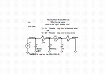
Below I show a thermal simulation that illustrates the voltage divider being driven by a current source. All temperatures are referred to ambient, which is thermal ground. In this simulation, there are three lumped thermal resistances: junction-to-header; header-to-sink; and sink-to-ambient. To make the numbers simple, all three thermal resistances are set to 0.8 C/W. It is not way off, by the way, to have almost 0.8 C/W thermal resistance from case to heat sink when a silpad insulator is used.
The junction has a fast time constant on the order of 17 ms, the header has an intermediate time constant on the order of a second, and the heat sink has a long time constant of about 40 seconds.
If you want to predict the junction temperature rise from the header temperature rise, the $64,000 question is whether you view the voltage divider as a 2:1 divider to the heat sink or a 3:1 divider to the ambient.
During medium time intervals, on the order of 1-10 seconds, when the heat sink temperature moves very little, the appropriate divider ratio is 2:1. However, for longer-term intervals, like 30 seconds to infinity, the 3:1 divider model is more appropriate.
In the former case (A) the predicted junction rise is 2 times the header rise. In the latter case (B) the predicted junction rise is 1.5 times the header rise. There is no right answer when the time dynamics are considered, given all the different time constants involved.
The simulation depicts a 14-watt power input, as modeled by 14 amps. The near-final junction rise over ambient is 33C at 100 seconds. I freely admit that I just guessed at the heat sink time constant.
At 3 seconds, Case A error is 0.7C and Case B error is –5.2C. At 100 seconds, Case A error is 10.4C and Case B error is –0.3C.
Cheers,
Bob
JPV said:
I understand that the power is a current source.
I you attack a resistive divider on the top with a current source, the voltage at middel of the divider will still be the voltage at the top multiplied by the dividing ratio.
The difference of the two temperatures increases with the power applied but their ratio remains constant ( the dividing ratio).
Therefore if we can measure one we know the other because we know the ratio.
Is this not correct?
JPV
Hi JPV,
Perhaps where we differ is in the intermediate time behavior as opposed to the static behavior at thermal equilibrium. Let me try to illustrate it in the voltage divider context that you have been using.
Below I show a thermal simulation that illustrates the voltage divider being driven by a current source. All temperatures are referred to ambient, which is thermal ground. In this simulation, there are three lumped thermal resistances: junction-to-header; header-to-sink; and sink-to-ambient. To make the numbers simple, all three thermal resistances are set to 0.8 C/W. It is not way off, by the way, to have almost 0.8 C/W thermal resistance from case to heat sink when a silpad insulator is used.
The junction has a fast time constant on the order of 17 ms, the header has an intermediate time constant on the order of a second, and the heat sink has a long time constant of about 40 seconds.
If you want to predict the junction temperature rise from the header temperature rise, the $64,000 question is whether you view the voltage divider as a 2:1 divider to the heat sink or a 3:1 divider to the ambient.
During medium time intervals, on the order of 1-10 seconds, when the heat sink temperature moves very little, the appropriate divider ratio is 2:1. However, for longer-term intervals, like 30 seconds to infinity, the 3:1 divider model is more appropriate.
In the former case (A) the predicted junction rise is 2 times the header rise. In the latter case (B) the predicted junction rise is 1.5 times the header rise. There is no right answer when the time dynamics are considered, given all the different time constants involved.
The simulation depicts a 14-watt power input, as modeled by 14 amps. The near-final junction rise over ambient is 33C at 100 seconds. I freely admit that I just guessed at the heat sink time constant.
At 3 seconds, Case A error is 0.7C and Case B error is –5.2C. At 100 seconds, Case A error is 10.4C and Case B error is –0.3C.
Cheers,
Bob
Attachments
Bob,
Here are the same thermal time constant test results performed on the 4xxx, but this time with the addition of a Bergquist Sil-Pad (A2000 material, 0.020" uncompressed thickness) pad between the transistor and the part. I estimate about 25-30 psi of clamping force....
Looks like the TC is a bit faster with the pad...
John
Attachments
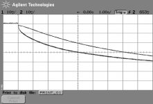
And last but not least, 7mA is still the magic If number for tansistor/diode matching at Ic=100 mA. In fact, with the sil-pad, tracking improves...
John
John
I tested tracking on one of JPV's units...
Here's the crux for the 3xxx series. I get near perfect tracking between Vbe on the transistor and Vf on the diode with Ic=100mA and diode If=0.5 to 3 mA with tracking being the best at around 2 mA.
You'll need to use more diodes in the diode string with the 3xxx than the 4xxx as the 3xxx Vf is quite a bit lower than Vbe: 0.45 and 0.62V respectively when tracking. This is mainly due to running the diode at lower currents.
The good news is that tracking seems to be marginally better with the 3xxx than with the 4xxx.
Cheers,
John
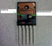
I've been busy today! I ground open one of my 4xxx ThermalTrak's... Here's what I found...
1) The diode and transistor are indeed separate devices bonded to a copper(?) backplate.
2) The transistor die is 0.250 x 0.250 in and is centered horizontally on pin 2 with an 0.020" offset to the right. Vertically, it's up 0.385" from the edge of the case (lead entry side).
3) The diode is centered horizontally over pin 4 and is also 0.385 in up from the edge of the case.
So, the diode isn't even in the transistor's thermal path! Just next to the transistor die. The center to center distance between the diode and transistor die is 0.250"
I'd take a picture, but...
1) I don't have a digital camera available right now.
2) I accidentally knocked the diode off the backplate leaving a bare area where it used to be. The diode shot off into lala land. I'm still sulking about that....
John
ditto!
very useful stuff here!
mlloyd1
very useful stuff here!
mlloyd1
Carl_Huff said:What a great thread!
Thank you for sharing so much!!
Here's a PSPICE model for the diode in the 4xxx that I tweaked to reflect reality. This model is for 27 degC only as I haven't been able to tweak the model sucessfully to model its behavior over temperature. I gave up on that...
.MODEL Dnjl4302dg_diode d
+ IS=5.5e-008 RS=0.65 N=2 TT=5.1937e-008 CJO=2.08272e-011 VJ=1.5+/n M=0.653713 EG=1.3 XTI=2.33354 BV=400 IBV=1e-005
John
.MODEL Dnjl4302dg_diode d
+ IS=5.5e-008 RS=0.65 N=2 TT=5.1937e-008 CJO=2.08272e-011 VJ=1.5+/n M=0.653713 EG=1.3 XTI=2.33354 BV=400 IBV=1e-005
John
jgedde said:Here's a PSPICE model for the diode
Excellent work! I have been using the NJL3281D/1302D and in simulation couldn't find a good fit diode model (wound up using some 1N4001 with some MUR1520). Your model is an exact match for the real performance I'm seeing with the actual amp.

Magnificent work John. My thanks for going to so much trouble to advance our knowledge. Especially the grinding!
The question was asked a while back as to how the response of the internal diode compared with the temperature rise on the top of the package. (Which has I think now been demonstrated to definitely be the best sensor position for non-TTrak transistors)
Time for a Yuletide experiment. In the attached screen-shot the diode voltage for a 5mA current is at the top, and the lower trace is the temperature at the top of the package as measured by an LM35 TO-92 temp sensor. Assuming -2mV/degC for the diode, both scales are 5 degC per large division. The power step was 6W, TTrak was on a sizable heatsink, thermal washer Koolpad K230 fitted between the TTrak top and the LM35.
The internal diode responds more and faster, no question there. Hmm!
Attachments
- Status
- Not open for further replies.
- Home
- Amplifiers
- Solid State
- On Semi ThermalTrak