THERMALTRAK TESTS 1
I have at last got round to acquiring some ThermalTraks, and doing a few hours work with them. And I am here to tell you that all our theoretical discussions appear to be well off the mark.
The test amplifier is an EF Type 2 and is essentially the Load-Invariant with the output stage converted from CFP to EF.
The maximum power was 20W/8R but the amplifier was run at 8.3W out to increase the dissipation.
The main heatsink is deliberately small to speed up heating and cooling; it got warm but not hot; using the Mk1 fingertip, I would say about 40 degC.
The driver heatsinks are large for the power level, to minimise driver heating and keep things simpler. They stayed at ambient temperature.
A solder mask has been dispensed with to make it easier to solder to tracks.
I used the method I mentioned here of underbiasing to about 0.03% and measuring the change in amplitude of the crossover spikes with time.
I have not had time to make pretty graphs of the data, so I'm afraid all I can show you is some screen-shots that are of less than stunning quality, but I hope they will show what's going on.
Since it appears you can only attach one pic per post, this will have to be in installments that I will number at the top.
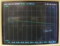
The first three tests use conventional compensation to establish a reference. The TTrak diodes were not used.
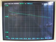
Test 1) Sensor transistor mounted on the driver heatsink.
There is an initial fast increase in bias, I assume- but do not know- that this is the output device junction heating.
There is then a steady increase over 200 seconds as the main heatsink warms up. The amplifier is seriously undercompensated.
I have at last got round to acquiring some ThermalTraks, and doing a few hours work with them. And I am here to tell you that all our theoretical discussions appear to be well off the mark.
The test amplifier is an EF Type 2 and is essentially the Load-Invariant with the output stage converted from CFP to EF.
The maximum power was 20W/8R but the amplifier was run at 8.3W out to increase the dissipation.
The main heatsink is deliberately small to speed up heating and cooling; it got warm but not hot; using the Mk1 fingertip, I would say about 40 degC.
The driver heatsinks are large for the power level, to minimise driver heating and keep things simpler. They stayed at ambient temperature.
A solder mask has been dispensed with to make it easier to solder to tracks.
I used the method I mentioned here of underbiasing to about 0.03% and measuring the change in amplitude of the crossover spikes with time.
I have not had time to make pretty graphs of the data, so I'm afraid all I can show you is some screen-shots that are of less than stunning quality, but I hope they will show what's going on.
Since it appears you can only attach one pic per post, this will have to be in installments that I will number at the top.
The first three tests use conventional compensation to establish a reference. The TTrak diodes were not used.
Test 1) Sensor transistor mounted on the driver heatsink.
There is an initial fast increase in bias, I assume- but do not know- that this is the output device junction heating.
There is then a steady increase over 200 seconds as the main heatsink warms up. The amplifier is seriously undercompensated.
Attachments
THERMALTRAK TESTS 2
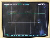
The sensor transistor was then moved to the main heatsink, to give conventional compensation.
Test 2) Sensor transistor mounted on the main heatsink, about 2cm from the edge of the output device.
The compensation is much better; somewhat overcompensated as the transistor Vbe is multiplied 4 times but the drivers are staying cold.
Attachments

THERMALTRAK TESTS 3
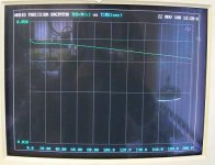
3) Sensor transistor mounted on top of one of the output devices.
The initial transient is now faster (10sec rather than 35sec) which is what I would expect. The long-term compensation is also good, though that is more luck than judgement- the amount of thermal coupling to the sensor happens to be about right.
This is intended to represent the best that conventional compensaton can do.
Attachments
THERMALTRAK TESTS 4
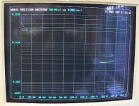
This is the first use of the TTrak diodes. They were simply put in series with the sensor Vbe-multiplier, which was turned down in voltage as it is now only compensating the drivers. The sensor was moved back to one of the driver heatsinks. The VAS current was 9.2 mA.
NOTE- the scale has changed.
The initial transient is now both smaller and faster, but over 200 seconds we are clearly undercompensated. This was no surprise as we know that the TTrak diode tempco at 9.2 mA is less than that of the transistor Vbe's.
More soon.
Attachments
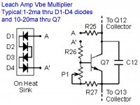
How well will the Leach-style Vbe multiplier work with ThermalTraks?
Most Leach designs typically have 1-2ma thru the diode string and 10-20ma through the Vbe multiplier transistor.
To built an optimally biased circuit, many designs require using fewer diodes between the base-collector than the total number of output transistors.
An experiment that can validate how well N-diodes in the Leach Vbe multiplier can compensate for K-output transistors using the ThermalTrak Tc factors would be very useful.
Attachments
THERMALTRAK TESTS 5
This is the second use of the TTrak diodes.
We worked out that the TTrak diode current needed to be much less (158uA) to give correct tempco matching. Here the TTrak diodes have been taken out of the VAS path and fed with 800 uA (for various reasons not 158uA) and their voltage drop added to the driver Vbe-multiplier.
The results are better than Test 4, but still undercompensated.
Attachments
THERMALTRAK TESTS 6
This is the third use of the TTrak diodes.
This time the TTrak diodes are once more passing about 9.2mA but their Vf is multiplied by a factor of two, and then added to the driver Vbe-multiplier. The long-term compensation is now good, though our theory says it should be quite seriously overcompensated as 2 x 1.7mV/degC = 3.4mV/degC, much more than 2.14mV/degC. There is also a rather worrying dip in the first 20 seconds- where does that come from?
That's all for now.
Douglas
Attachments

DouglasSelf said:THERMALTRAK TESTS 6
This is the third use of the TTrak diodes.
This time the TTrak diodes are once more passing about 9.2mA but their Vf is multiplied by a factor of two, and then added to the driver Vbe-multiplier. The long-term compensation is now good, though our theory says it should be quite seriously overcompensated as 2 x 1.7mV/degC = 3.4mV/degC, much more than 2.14mV/degC. There is also a rather worrying dip in the first 20 seconds- where does that come from?
That's all for now.
Douglas
I am really surprised by this experiment.
Initial questions to check if I understand well:
Would it not be normal that the distortion would drop ( therefore the dip) and then go back to 0.03% if the tracking is perfect long term?
I do not understand why this bias in the distortion in case of good tracking
Did you adjust for 0.03% distortion at low dissipation or at max dissipation?
I would have an explanation if the experiment would have been with overbias and not underbias..; too bad
JPV
Juergen Knoop said:Douglas I'm puzzled, isn't test#1 that with the lowest thd? 😕
regards
It ends up at the lowest THD, but that is because it is so badly undercompensated that the bias shows the biggest increase. The important point is not the actual THD figure, but how it changes over the test period.
Douglas
JPV said:
I am really surprised by this experiment.
Initial questions to check if I understand well:
Would it not be normal that the distortion would drop ( therefore the dip) and then go back to 0.03% if the tracking is perfect long term?
I do not understand why this bias in the distortion in case of good tracking
Did you adjust for 0.03% distortion at low dissipation or at max dissipation?
I would have an explanation if the experiment would have been with overbias and not underbias..; too bad
JPV
He did't adjust the amp for lowest THD but for some I bias and he look at variation of crossover distortion with temperature. A straight line in THD measurement imply zero delta I bias 😉
Question for sir Douglas Self:
As we well known, a ring emitter BJT has some parasitic BE resistance, which add to the external one (Re) in a standard EF output stage. What is the optimum VRe for minimum crossover distorsion in the case of ThermalTrack devices?
Thank you,
Mihai
JPV said:
I am really surprised by this experiment.
Initial questions to check if I understand well:
Would it not be normal that the distortion would drop ( therefore the dip) and then go back to 0.03% if the tracking is perfect long term?
I do not understand why this bias in the distortion in case of good tracking
Did you adjust for 0.03% distortion at low dissipation or at max dissipation?
I would have an explanation if the experiment would have been with overbias and not underbias..; too bad
JPV
No. If the tracking was perfect then the THD would be constant, a dead flat line.
The amplifier dissipation was always the same. I switch on, set the THD to roughly 0.03%, (you can't set it exactly as it is changing while you do it) switch off and cool it down with a fan, then switch on and start the test from the cold state.
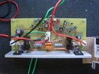
This is the amplifier, with the sensor on the right-hand driver hsink.
Attachments
DouglasSelf said:
No. If the tracking was perfect then the THD would be constant, a dead flat line.
The amplifier dissipation was always the same. I switch on, set the THD to roughly 0.03%, (you can't set it exactly as it is changing while you do it) switch off and cool it down with a fan, then switch on and start the test from the cold state.
This is the amplifier, with the sensor on the right-hand driver hsink.
I am discussing the non Thermaltrack experiment first
I understand that the THD should be flat in time but should it not then be at 0,03% when the tracking ( supposed perfect) has brought the bias back to its steady state condition?
During the transient after switch on, it is normal that THD should plunge because the Vbias in the cold state is higher than in the hot steady state therefore the Vq is higher which means THD lower . Then tracking will bring the steady state condition and THD should go back to 0.33% and stay there. Is this correct?
JPV
Douglas, Which ThermalTrak transistors did you use? It seems there are different diode VI curves and different diode SPICE models for the 4281/4302 and the 3281/1302.
If the datasheets are to be trusted, the 3281 diodes need flea currents to match tempcos. The 4281 matches tempco at around 7 mA.
OnSemi doesn't have stock on 4281s until March '09 si I'll have to wait 'til then to verify this...
Great work!
john
If the datasheets are to be trusted, the 3281 diodes need flea currents to match tempcos. The 4281 matches tempco at around 7 mA.
OnSemi doesn't have stock on 4281s until March '09 si I'll have to wait 'til then to verify this...
Great work!
john
JPV said:
I am discussing the non Thermaltrack experiment first
I understand that the THD should be flat in time but should it not then be at 0,03% when the tracking ( supposed perfect) has brought the bias back to its steady state condition?
During the transient after switch on, it is normal that THD should plunge because the Vbias in the cold state is higher than in the hot steady state therefore the Vq is higher which means THD lower . Then tracking will bring the steady state condition and THD should go back to 0.33% and stay there. Is this correct?
JPV
I'm not sure I understand your question- if the tracking was perfect, the THD wouldn't be plunging or doing anything else. It would be constant, in both the short term and the long term.
Douglas
jgedde said:Douglas, Which ThermalTrak transistors did you use? It seems there are different diode VI curves and different diode SPICE models for the 4281/4302 and the 3281/1302.
If the datasheets are to be trusted, the 3281 diodes need flea currents to match tempcos. The 4281 matches tempco at around 7 mA.
OnSemi doesn't have stock on 4281s until March '09 si I'll have to wait 'til then to verify this...
Great work!
john
Thank you for your kind words! I used the 3281/1302 pair.
These were obtained from DigiKey, who most efficiently shipped them to me in the UK, in less than 48 hours.
I haven't gone into the issue, but I gather there is some doubt about the SPICE models for these devices. Do you have any recommendations?
Douglas
roender said:
He did't adjust the amp for lowest THD but for some I bias and he look at variation of crossover distortion with temperature. A straight line in THD measurement imply zero delta I bias 😉
Question for sir Douglas Self:
As we well known, a ring emitter BJT has some parasitic BE resistance, which add to the external one (Re) in a standard EF output stage. What is the optimum VRe for minimum crossover distorsion in the case of ThermalTrack devices?
Thank you,
Mihai
Well, it is a good question, but more than a bit off-topic here. My thoughts on this are on p152-154 of the 4th Edition of the Audio Power Amplifier Design Handbook.
DouglasSelf said:
I haven't gone into the issue, but I gather there is some doubt about the SPICE models for these devices. Do you have any recommendations?
Andy_c made these models for the non-TT versions that seem accurate:
.MODEL MJL1302A_X pnp IS=9.8145e-12 BF=122.925 NF=1.00 VAF=40 IKF=19 ISE=9.18577762370362E-07 NE=5.0 BR=4.98985 NR=1.09511 VAR=4.32026 IKR=4.37516 ISC=3.25e-13 NC=3.96875 RB=3.30 RE=0.00 RC=0.06 XTB=0.115253 XTI=1.03146 EG=1.11986 CJE=1.561e-08 VJE=0.781803 MJE=0.433868 TF=3.257e-9 XTF=1000 VTF=2.0 ITF=260 CJC=2.346838e-9 VJC=0.27876 MJC=0.411324 XCJC=0.959922 FC=0.1 CJS=0 VJS=0.75 MJS=0.5 TR=1e-07 PTF=0 KF=0 AF=1 Vceo=200 Icrating=15 mfg=OnSemiconductor
.MODEL MJL3281A_X npn IS=9.8145e-12 BF=438.0 NF=1.00 VAF=38 IKF=19.0 ISE=1.0e-12 NE=1.1237388682 BR=4.98985 NR=1.09511 VAR=4.32026 IKR=4.37516 ISC=3.25e-13 NC=3.96875 RB=3.997 RE=0.00 RC=0.06 XTB=0.115253 XTI=1.03146 EG=1.11986 CJE=1.144e-08 VJE=0.468574 MJE=0.34957 TF=2.6769e-9 XTF=7500 VTF=3.0 ITF=1000 CJC=1.093685e-9 VJC=0.623643 MJC=0.482111 XCJC=0.959922 FC=0.1 CJS=0 VJS=0.75 MJS=0.5 TR=1e-07 PTF=0 KF=0 AF=1 Vceo=200 Icrating=15 mfg=OnSemiconductor
DouglasSelf said:
I'm not sure I understand your question- if the tracking was perfect, the THD wouldn't be plunging or doing anything else. It would be constant, in both the short term and the long term.
Douglas
OK
When I say perfect tracking I mean perfect perfect equality of temco of Vbias and output transistors. But there is always a thermal delay between them due to size of chip, package, mounting and so on. What I am asking then is: is it not normal to have this dip at the start due to this inevitable delay even if in steady state they track perfectly. It seems to me that the base emitter junction of the Vbias transistor will be cooler than the junction of the output transistor at the start for a short transient time. During that time Vbias will be higher and therefore distortion smaller
My second question is : how do you explain the fact that it has to be way overcompensated to have the TT transistors tracking well. Does thsi mean that the announced temco is wrong?
JPV
- Status
- Not open for further replies.
- Home
- Amplifiers
- Solid State
- On Semi ThermalTrak