sorry , even if I'm immensely enjoying drawing my own ...... I'm feeling terrible even looking at someone else's pcbs ; most probably just tired of years of service , when deciphering schematic from physical layout is daily routine
hope somebody will chime in
hope somebody will chime in
Hi All,
Finally starting to implement my M2 PCB inside the amplifier box,
i would like to protect the circuit against peak at power up and inrush currents.
attached in folowing picture, the location of the CL-60!
i am not sure if it is the best position!
also some caps to absorb the peaks at power!
any caps to recommend ?
and is the CL-60 (5A) the best choice?
your expertise would be more than welcome !
thanks in advance!
An externally hosted image should be here but it was not working when we last tested it.
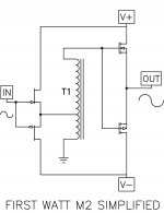
CL60 - one in primary
second CL from central GND point (bridge between to cap pcbs) to chassis
chassis connected to safety GND
second CL from central GND point (bridge between to cap pcbs) to chassis
chassis connected to safety GND
sorry, been out for lunch.
next question!
I've been able to obtain some FQA12P20/19N20 but their VGS is some 1.5V apart (Ps from Ns).
Butttttt....
I found some old IRFP140/9140 in my drawer wich match perfectly at 4V.
So...
would it be beneficial to apply the later in M2 circuit??
faithfully A.
next question!
I've been able to obtain some FQA12P20/19N20 but their VGS is some 1.5V apart (Ps from Ns).
Butttttt....
I found some old IRFP140/9140 in my drawer wich match perfectly at 4V.
So...
would it be beneficial to apply the later in M2 circuit??
faithfully A.
put whichever please you ...... even if matching N vs. P is of zero relevance
it's nice to have two input JFets matched
it's nice to have two input JFets matched
I looked around 'cause Teabag mentioned Vishay/Siliconix 9240 to be bad in this circuit.
so I put the uneven FQAs in and spare my old IRFPs for a project where matching is obligate.
thanx, ZM
A.
so I put the uneven FQAs in and spare my old IRFPs for a project where matching is obligate.
thanx, ZM
A.
hundred men , hundred and ten tastes , two hundred titties .......... 
I'm finding Vishay P channel so sexy ...... 🙂
I'm finding Vishay P channel so sexy ...... 🙂
@Fabian85, you've got some room to fatten up a couple of your traces. In particular, I'd fatten the ones between the MOSFETs and R13/R14, but also those between V+ and V- and the MOSFETs.
It wouldn't hurt to make the input traces around R1 and the transformer smaller so they don't inadvertently pick up noise.
If your V+ to C3 trace is in the top copper, then I don't know how reasonable it is to rely on the solder mask for electrical isolation with the heatsink. You could cover it with Kapton tape, but it might be easier to make sure any under-heatsink traces are in the back copper.
Cheers,
Jeff.
CL60 - one in primary
second CL from central GND point (bridge between to cap pcbs) to chassis
chassis connected to safety GND
+1 on moving the CL-60 to the primary side of the transformer. The transformer has a lot of inrush itself and will force the use of a larger fuse with the CL-60s on the secondaries.

Another file adding sizes...
I strongly suspect those holes are 50.8mm (2") apart, rather than 50mm....
Cheers altogether,
...a friend of mine who owns an original F5. ... thinking of making some M2 Boards to swap out in his current F5 amplifier,...
Fabian
You are funny. Rip apart an org.F5
Hi All ,
for the IRFP240 and IRFP9240, what thermal interface product do you recommand ?
I have few option in stock in my drawer:
some aluminium oxide pads, silicon pads, probably also some mica pads.
what about the thermal grease or paste something to recommand with these pads?
with the hard pads as the aluminum oxyde or mica , some paste is clearly needed , but for the silicon pad probably not thermal paste is requiered?
thanks in advance
An externally hosted image should be here but it was not working when we last tested it.
Last edited:
Syl20M
Re thermal pads
It’s best to use the Keratherm from the store
Keratherm Transistor Insulators – diyAudio Store
Unless the ones you have are of equal specs
FR
Re thermal pads
It’s best to use the Keratherm from the store
Keratherm Transistor Insulators – diyAudio Store
Unless the ones you have are of equal specs
FR
+1 for mica + goop.
Other than the potential bit of messiness the goop poses, it works perfectly for me.
Even for more than 40W per MOSFET in TO-247 ...
Best regards,
Claas
Other than the potential bit of messiness the goop poses, it works perfectly for me.
Even for more than 40W per MOSFET in TO-247 ...
Best regards,
Claas
- Home
- Amplifiers
- Pass Labs
- Official M2 schematic