The original M2 has a regulated power supply. However, the build threads here don't seem to suggest regulated supplies in clones.
Are you sure? I cannot see any active regs inside
absolutely not
I too had a good look at the pictures on 6moons and didn't see any regulated supply. But this line from http://www.firstwatt.com/pdf/prod_m2_man.pdf is what prompted me to guess so, "It takes about 1 minute for the regulators to come up to full voltage, so don’t expect full output power for that time." (page 7).
well , he made it , he can write whatever he want 
besides , it's much easier (and better sounding/impressing) to write "regulators" than to write entire sentence instead :
"due to limiting action of resistors connected in series to bibadasscap in biasing circuit, cap itself is filling with juice pretty slowly , so you can go and do your dinner , while amp is slowly starting to sing"
see - much simpler , and it probably saves Tree ....... (or two)

well , he made it , he can write whatever he want
besides , it's much easier (and better sounding/impressing) to write "regulators" than to write entire sentence instead :
"due to limiting action of resistors connected in series to bibadasscap in biasing circuit, cap itself is filling with juice pretty slowly , so you can go and do your dinner , while amp is slowly starting to sing"
see - much simpler , and it probably saves Tree ....... (or two)

🙂
While we are at it, what is the Bias current per Mosfet, as per standard M2 circuit? Thanks.
P.S. I am asking because I played music through the M2 Output Stage with a different line driver circuit; it played beautifully until the Source resistors caught fire. Hence, I changed the damaged components and changed the Source resistors to 1.1 ohms (3.3R x 3 in parallel). The bias current is racing away beyond 2 amps per rail with 23.5 Volts DC rails.
P.S. I am asking because I played music through the M2 Output Stage with a different line driver circuit; it played beautifully until the Source resistors caught fire. Hence, I changed the damaged components and changed the Source resistors to 1.1 ohms (3.3R x 3 in parallel). The bias current is racing away beyond 2 amps per rail with 23.5 Volts DC rails.
something is pretty ooked in your case
name of the game is biasing circuit doing everything it can , to maintain aroundish 1V1 across two mosfet source resistors (in series) ..... so with 0R94 that's something as 1A2 ...... and with spread here and spread there , everything up to 1A5 is normal
post exact schm you're using ( everything left from 10uF cap is irrelevant) and few pictures , if possible
check all resistors values
He means Q6 & Q7. LM385 are shunt regulators and due to C3 it takes some time until bias voltage rises up to its final value.I too had a good look at the pictures on 6moons and didn't see any regulated supply. But this line from http://www.firstwatt.com/pdf/prod_m2_man.pdf is what prompted me to guess so, "It takes about 1 minute for the regulators to come up to full voltage, so don’t expect full output power for that time." (page 7).
nope
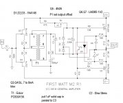
LM385 are there for safeguarding duty (so no chance that opto-diode goes poof)
you can go without them ....... or change with 1V25 zenners ...... if you find them 🙂
try to analyze circuit without any diode - it'll work
then add one by one , and you'll find what each one is used for
LM385 are there for safeguarding duty (so no chance that opto-diode goes poof)
you can go without them ....... or change with 1V25 zenners ...... if you find them 🙂
try to analyze circuit without any diode - it'll work
then add one by one , and you'll find what each one is used for
Last edited:
LM385's have important function that is not protection.
The 1.2V shunt reg is balanced off against the 1.2V forward bias of the
opto, and keeps the bias circuit from reacting to output current much greater
than the bias current.
This way you can go into Class AB mode with low impedance loads without
creating problems.
Without it, a high current transient would be interpreted as high bias, and
would drain the capacitor, requiring some time to recover.

I stand corrected

(though , I'm going to call them limiters , which I meant ..... but was either too dumb or clumsy to use proper term ; most probably just dumb)

(though , I'm going to call them limiters , which I meant ..... but was either too dumb or clumsy to use proper term ; most probably just dumb)
After examining my build, I finally found the problem. I followed the schematic in post 39 of this thread (Official M2 schematic) wherein the Base of the transistor in the Optocoupler is connected instead of the Collector. Need to make modifications in the home etched PCB to verify M2's proper working now.
Though, in the meantime the Schade feedback simulations over in this thread Most Greedy Boy, of them all... or (there is no) DEFiSIT of Papa's Koans are very interesting, I will forge ahead.
Thank you ZM for your inputs.
Though, in the meantime the Schade feedback simulations over in this thread Most Greedy Boy, of them all... or (there is no) DEFiSIT of Papa's Koans are very interesting, I will forge ahead.
Thank you ZM for your inputs.
damn
next time you'll know better - always use original schm .......
🙂
let us know outcome .......... though , I couldn't wait no longer than Pronto! to redo the pcb and try .....
next time you'll know better - always use original schm .......
🙂
let us know outcome .......... though , I couldn't wait no longer than Pronto! to redo the pcb and try .....
M2 frontend is sounding Mega Giga Super nice, as frontend for a headphone amp 🙂
I combined it with the upcoming DIY Headphone amp output stage and it's a keeper...
So I made a quick PCB, found some old Teko TK3710 RF-cases for shielding the Edcor's and the M2 Headphone amp is born 😀
Strange....I always hated the combination of transformers and audio...but I was so wrong... CSX1, F6 and now M2 they all sound so nice.
Makes me wonder how the M2 sounds on my big loudspeakers... 😱
I have finished my M2 HA (thanks Walter, Nelson and Wayne) but I don´t see that the optocoupler cancels the Offset. Any idea how I can solve it? 😕
Still not a feedback (no signal is being fed back there) but a voltage divider that makes MOSFET's Id dependable on Vds which changes its output characteristic into triode looking one....the Schade feedback simulations over in this thread ...
Help on new M2 build
Merry Christmas!
Every Christmas vacation, I end up building one amp from Papa. This Christmas I set about making a M2 using an existing F5 chassis. The boards are from Grimberg group buy.
Used light bulb to test out each channel and things are fine. No short or anyu other smoke.
Both the channels show up a +ve offset at the output of around 3V (yes volts) and not able to get it to zero on either side of the offset adjustment trimpot.
I am using some random Toshiba 2SJ201/2SK1530 pair (not matched). Could the offset be so much due to big possible variation on VGS of the Mosfet pair?
I do have close matched IRFs which I bought for F4 build (IIRC). Should I try that option or adjust the R6/R7 values? I am baffled by this large offset.
There are no parts getting heated up other than R13/R14s getting warm.
Need suggestions/advice on reducing the offset.
Thanks in advance.
Cheers
Anil
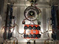
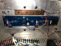
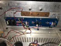
please post actual schematic and pictures of build
write down what is voltage across source resistors , what is exact (minimal) DC offset you can get with trimpot on end , taking care of proper polarity (probes)
then we can help with more specific steps
write down what is voltage across source resistors , what is exact (minimal) DC offset you can get with trimpot on end , taking care of proper polarity (probes)
then we can help with more specific steps
- Home
- Amplifiers
- Pass Labs
- Official M2 schematic


