optocoupler is there , functioning in this way:
LED is fed with voltage across two source resistors
series resistor for LED is to keep current and voltage for LED in safe area
LED is shinin' on transistor base , defining conductivity through it
transistor is part of current path from + to - PSU rails , and it's maintaining proper voltage between mosfet gates
(current through mosfets rise , LED shining brighter , transistor more open/lesser effective resistance , so lesser voltage between gates so current through mosfets decline)
3300uF across transistor is to neutralize process of normal current fluctuation through mosfet source resistors , so LED is having in same manner fluctuating voltage , inducing same fluctuating of light to transistor base
that way voltage between mosfet gates is held pretty solid and steady
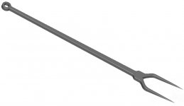
so imagine that cap as wide open solid fork ,placed with fork pins between two gates
on whichever side (pin) of fork you're pushing/pulling , other side is following , always staying exactly same apart
in case of M2 , fork is pushed/pulled on lower end , through C2
you can connect it to other end of C3 , result will be the same
I bypassed C3 with 1uF polycarbonate just because I can , will sleep like a baby , knowing that I'm done everything that fork stays solid even on highest frequencies**
that's exactly intended role of C3 - to not conduct signal , but to represent solid pushrod to signal ; that trick/part of circ is sometimes called level shifter
**not that's for certain , but sleep is important
(all ref. to schm in post #1 ; sketch of exact forks missing there , so I'm enclosing it , just in case ; second picture just because I'm Enormous and my Ego is Enormous)

edit: linked schm from #13 , so you don't need to jump from tab to tab :
LED is fed with voltage across two source resistors
series resistor for LED is to keep current and voltage for LED in safe area
LED is shinin' on transistor base , defining conductivity through it
transistor is part of current path from + to - PSU rails , and it's maintaining proper voltage between mosfet gates
(current through mosfets rise , LED shining brighter , transistor more open/lesser effective resistance , so lesser voltage between gates so current through mosfets decline)
3300uF across transistor is to neutralize process of normal current fluctuation through mosfet source resistors , so LED is having in same manner fluctuating voltage , inducing same fluctuating of light to transistor base
that way voltage between mosfet gates is held pretty solid and steady
so imagine that cap as wide open solid fork ,placed with fork pins between two gates
on whichever side (pin) of fork you're pushing/pulling , other side is following , always staying exactly same apart
in case of M2 , fork is pushed/pulled on lower end , through C2
you can connect it to other end of C3 , result will be the same
I bypassed C3 with 1uF polycarbonate just because I can , will sleep like a baby , knowing that I'm done everything that fork stays solid even on highest frequencies**
that's exactly intended role of C3 - to not conduct signal , but to represent solid pushrod to signal ; that trick/part of circ is sometimes called level shifter
**not that's for certain , but sleep is important
(all ref. to schm in post #1 ; sketch of exact forks missing there , so I'm enclosing it , just in case ; second picture just because I'm Enormous and my Ego is Enormous)
edit: linked schm from #13 , so you don't need to jump from tab to tab :
Attachments

Last edited:
If we want to drive the amp directly with just an attenuator in front of the buffer, we just replace R2 with 1M and attach an 25K pot in front of it?
Do we also have to bring R1 inside of R2?
Do we also have to bring R1 inside of R2?
leave them both in , just change 100K to 1M
why should I ever believe some crapy pot , to establish gnd potential for my precious gate/grid ?
why should I ever believe some crapy pot , to establish gnd potential for my precious gate/grid ?

M2 sez : why should I care ?
you can use 10K ,if all sources you're using are able to drive it ..........
you can use 10K ,if all sources you're using are able to drive it ..........


What do you think?
@ Dimkasta
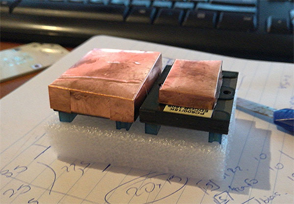
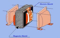
Good try 🙂 You can make multilayers transformer shield protections with copper tape first .
The best solution bend tape all around without shorts or contacts with wire inputs or outputs windings
With close in mu metal can after that you don't be worry about cosmic radiations from Alpha Centauri as well

Attachments
-
 BE5BA385-0B5A-42B5-8C10-C53067081393.JPG45.5 KB · Views: 300
 -
 66F2CA8E-A11C-41BE-A782-965895EEA7AA.JPG50.8 KB · Views: 789
 -
 92CD8C7B-F1B4-4737-BA6A-7736DC87427A.JPG564.6 KB · Views: 798
 -
 3E1C3CA5-A014-47D0-A1EA-C167F506A2AE.JPG815.3 KB · Views: 832
 -
 B8A636D9-23EA-4512-9F9A-D3C433D68FF3.JPG24.2 KB · Views: 304
 -
 40096301-C753-4747-A945-77786657CFA2.JPG25.2 KB · Views: 284
if you have higher Idss range ones (more than , say , 8mA) , just check their current in circ , measuring voltage drop across R3 and R4 (ref. to post #1)
increase R3 and R4 if needed
I found a set of 8 idss I think will be fine, thanks for the info guys!
Russellc
@ Dimkasta
Good try 🙂 You can make multilayers transformer shield protections with copper tape first .
The best solution bend tape all around without shorts or contacts with wire inputs or outputs windings
With close in mu metal can after that you don't be worry about cosmic radiations from Alpha Centauri as well
Thanks for the tip
I have made MuMetal boxes already but I will also add some copper tape as in the lower photos in your post
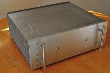
FirstWatt M2 Clone Done.
Happy New Year diyers.
Finally to get the amp up and running, bias set to 630mV, R13,14 on TeaBag's boards use 0.5ohms will draw about 1.26A. DC offset only able to get to 5mV because my part bin run out of certain value that will give me a more closer zero offset, may be do it next time.
The case dimensions approximately 17" width, 5.5" height and 14.75" depth. Heat sinks use 5.375"x14" from Heatsink USA, face plate 17"x6"x0.5" others just 16 gauge 6061H36 plate, all from local raw material shop.
I like the sound of the amp, it is my cup of tea. I am just a music lover don't know how to use the juicy words but it is absolutely worth the time and every single penny that you spend on it.
Thank you to NP's generosity, Choky's and fellows info., TeaBag's boards and Spencer's close match jfets.
Attachments
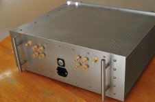
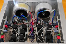
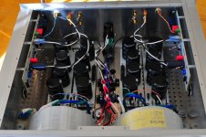
Fugly!
(put both bottom and top plate on 10mm spacers , you'll get much cooler inside of amp)
(put both bottom and top plate on 10mm spacers , you'll get much cooler inside of amp)
Yes, all the holes drilled by a floor stand drill press.
Will consider add an exhaust fan. BTW, I miss your stone grill sausages.
Will consider add an exhaust fan. BTW, I miss your stone grill sausages.
- Home
- Amplifiers
- Pass Labs
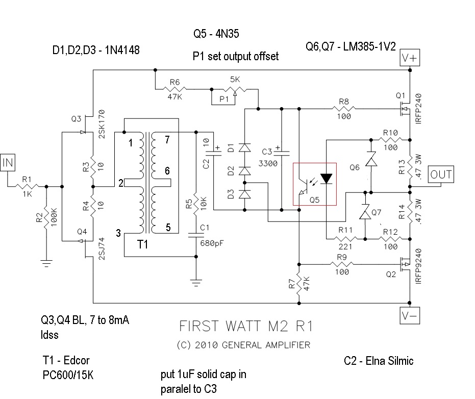
- Official M2 schematic