Status
I have updated the signup sheet indicating those who have already paid. If your name is not marked, one of two things happened:
1) The net funds received are less than what you should have paid
2) You forgot to provide the name you used in the signup sheet
In both cases I have already sent emails communicating the problem.
For members outside the USA, it seems as if the foreign exchange fee is 1%, which makes the total PayPal fees: 3.99% + $0.30
Members who signed up for the Group Buy and have not yet paid, must do it by 6:00 PM PST tomorrow, Sunday 1/24/2016. I am planning to place the order shortly after that so it will be in the queue for revision and processing at the beginning of the work day on Monday.
Paid $75 USD as of just now. I did the math and that should be slightly over, but in case I got it wrong, please let me know 🙂
Thanks again!
Thanks again!
Last edited:
Generg, you may have a point there: the DC drifts when I touch the supply clips. Will mount proper cables tomorrow.
Firmed up the power supply cabling and now the DC drift is within +-10mV.
I have the hunch that the remaining erratic drift comes in from the mains, very difficult to establish this in measurement, though.
The absolute Vgs in my FQA devices differ by almost 2V, so there is a chance that changes in supply voltage convey to the output DC.
Now that boards are ordered, if anymore comments are coming on BOM please make them soon.
Will update Google sheet soon
Dave
Sent from my C6606 using Tapatalk
Will update Google sheet soon
Dave
Sent from my C6606 using Tapatalk
Made an extra payment..
I urge you to review my original email and your math. You are still short.
I have the hunch that the remaining erratic drift comes in from the mains, very difficult to establish this in measurement, though.
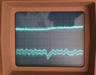
Attached a shot from my scope to back up my hypothesis. Bottom trace is positive rail (AC coupled, 50mV/Div), top trace is output (DC coupled, 20mV/Div). Time scale is .5s/Div.
In the middle of the screen there seems to be a drop in supply voltage by 50mV or so, followed by a recovery of the beam position due to the coupling capacitor of the scope. At the same position the output DC starts to rise.
Maybe you find this interesting.
Attachments
Hmm, I find it interesting!
Itd be easy to check if its mains variation though surely? Just check the mains voltage every once in a while and see?
Itd be easy to check if its mains variation though surely? Just check the mains voltage every once in a while and see?
One more comment about the BOM .... If you go to Mouser, there are SR 6/7 in the BOM, these are the resistors that may be needed if you cannot get the Bias to set.
See this post:
http://www.diyaudio.com/forums/pass-labs/281520-official-m2-schematic-59.html#post4590665
Please keep in mind that this BOM still has two caps on the bottom line that I need for another project.
The google spreadsheet is missing the extra resistors.
Dave
See this post:
http://www.diyaudio.com/forums/pass-labs/281520-official-m2-schematic-59.html#post4590665
Please keep in mind that this BOM still has two caps on the bottom line that I need for another project.
The google spreadsheet is missing the extra resistors.
Dave
The offset of an M2 will drift with supply some mV due to the mismatch
of Vgs of the N channel vs P Mosfets. The pot is meant to trim that, but
if you do the math, some dependency on ps voltage remains.
You can regulate the voltages feeding current to the bias circuit if you like.
😎
of Vgs of the N channel vs P Mosfets. The pot is meant to trim that, but
if you do the math, some dependency on ps voltage remains.
You can regulate the voltages feeding current to the bias circuit if you like.
😎
This is well noted Nelson.
Do we need to change value of R6 & R7 if we use Toshiba 2SK1530/2SJ201 for Q1 & Q2 ? What value? I understand they have slightly lower Vgs requirement than IRF mosfets.
Also, I'd like to put few naked Vishay resistors to your very nice design - will there be advantage and which part are these?
Do we need to change value of R6 & R7 if we use Toshiba 2SK1530/2SJ201 for Q1 & Q2 ? What value? I understand they have slightly lower Vgs requirement than IRF mosfets.
Also, I'd like to put few naked Vishay resistors to your very nice design - will there be advantage and which part are these?
Last edited:
This is well noted Nelson.
Do we need to change value of R6 & R7 if we use Toshiba 2SK1530/2SJ201 for Q1 & Q2 ? What value? I understand they have slightly lower Vgs requirement than IRF mosfets.
Also, I'd like to put few naked Vishay resistors to your very nice design - will there be advantage and which part are these?
Good question I plan to use those Toshiba devices to.
Greetings
This is well noted Nelson.
Do we need to change value of R6 & R7 if we use Toshiba 2SK1530/2SJ201 for Q1 & Q2 ? What value? I understand they have slightly lower Vgs requirement than IRF mosfets.
Also, I'd like to put few naked Vishay resistors to your very nice design - will there be advantage and which part are these?
no need to change anything
Vishay's - there is so many resistors , so you can put them in all positions

Hmm, I find it interesting!
Itd be easy to check if its mains variation though surely? Just check the mains voltage every once in a while and see?
I am looking for variations of 50mV/22V, i.e. 2 ‰. My simple volt meter doesn't do that.
Which of the FQA gave lower Vgs? If it is the N, you may try compensating using 2-3 1N4148 diodes or a green LED in series with P1. Or, you may use the Toshiba 2SJ201 and 2SK1530, they exhibit Vgs difference of about 300mV at 1.3A Id.The absolute Vgs in my FQA devices differ by almost 2V, ...
Which of the FQA gave lower Vgs? If it is the N, you may try compensating using 2-3 1N4148 diodes or a green LED in series with P1. Or, you may use the Toshiba 2SJ201 and 2SK1530, they exhibit Vgs difference of about 300mV at 1.3A Id.
Cunning! I might try that. Unfortunately the LED won't light up...
Voltage regs would be simple, too, but more parts I'd need to cram in. And I don't have any at hand.
My FQAs have Vgs = 3.74 V for the N channel and Vgs = -5.62 V for P, measured in situ.
I have Toshibas as well, and if I find the time I'll drop them in later today.
Last edited:
- Home
- Amplifiers
- Pass Labs
- Official M2 schematic