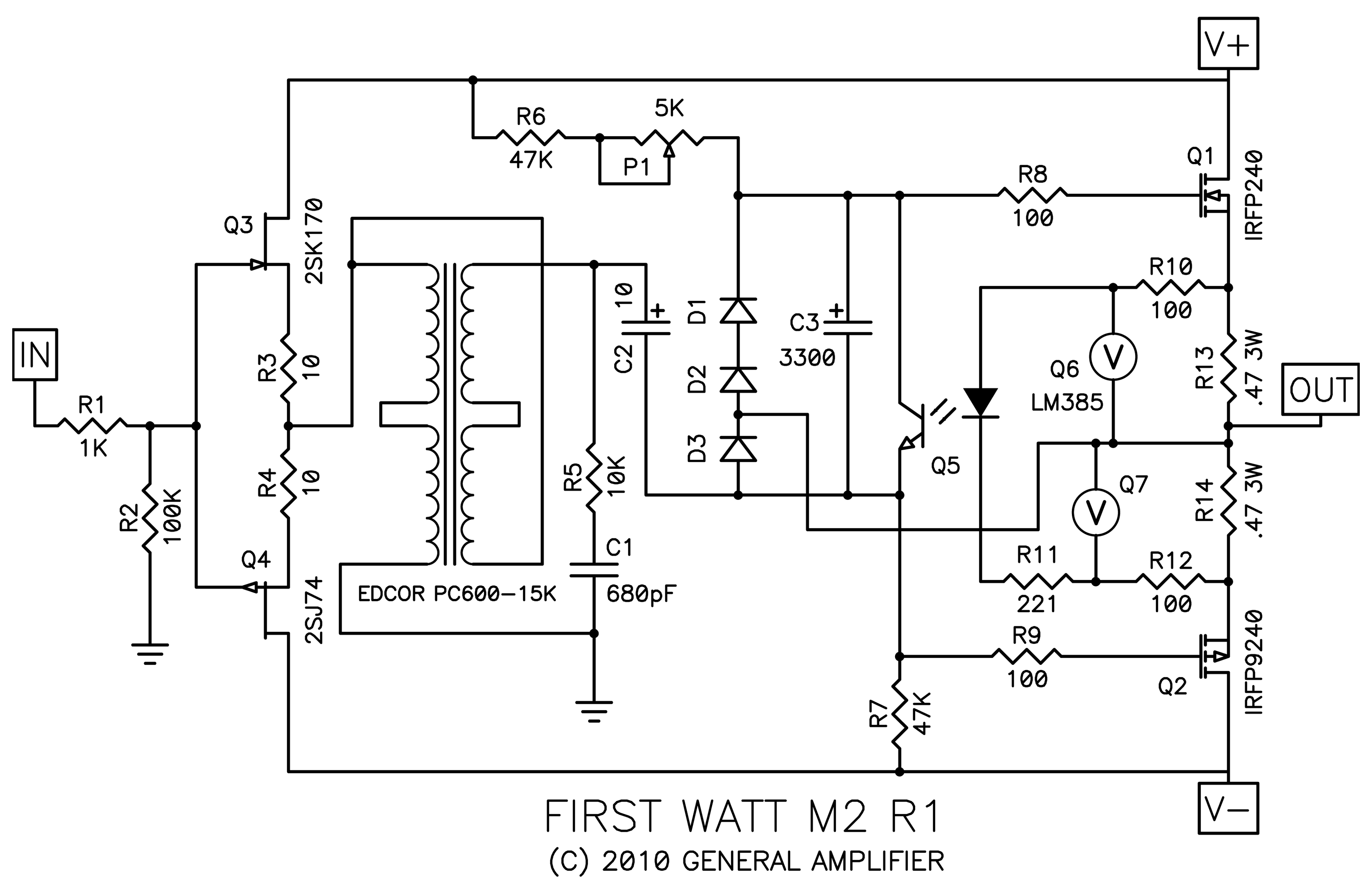
you can do the math:
The supply voltage drops from V+ over the n-FET, R13+R14, and the p-FET to V-, total drop some 45V.
Running at a bias of 1.5A (according to ZM) R13+R14 will drop ca 1.5V.
The data sheet of the FETs will tell you the Vgs necessary for that 1.5A, and remember that the Vgs of a p-FET is negative.
R6 and P1 need to drop the voltage from V+ to Vg(n-FET), and R7 needs to drop from Vg(p-FET) to V-. Between Vg(n-FET) and Vg(p-FET) the optocoupler will drop the two Vgs you read off the data sheet and the 1.5V over R13+R14.
Added the 3W R13 and R14
Been sticking with 5% rather than 1%, build a Pete Millett Starving student with the 5% rather than the 1%, and could not really hear anything bad, and did a bunch of reading and, not to start the debate all over, but it seems that there is still disagreement!
Dave
wirewound are usually avoided for their inductance
I suggest the following alternate values for R6: 49K9 for a 5% increase in the adjustment range and, if not enough, 52K3 for a 10% increase in the adjustment range.
71-RN60D-F-49.9K
71-RN60D-F-52.3K
71-RN60D-F-49.9K
71-RN60D-F-52.3K
[from zen Mod]
or value of resistor in series with pot
If I could get some input on these values, it would help me greatly. Unlike some DIY folks, I do not have a "parts bin" So, the marginal cost of a few resistors and a different value pst is often a week in lost time, and 10 times the value of the parts in shipping!
The answers are certainly in the F5 thread, and in fact, I remember scanning them, finding them is another matter
Thanks for the help
Dave
well , if said resistor is 47K , then you need to stash few lower standard values in drawer , same as few higher
do the math
being in this hobby , it's wise to invest in resistor packages , having at least 10pcs of each in , say, E12 range (going from 1R to 1M)
it's not that expensive and it will save you few headaches in very short time
Resistor Values E6 E12 E24 E48 E96 E192
if I remember correctly - I finished having 68K in place of R6 .......
generally - if fiddling with pot can't shave positive output offset , increase R6 to first higher value (higher than sum of R6 and P1) , so 56K or 62K , or 68K in case of needing more change
same applies for R7 value , if output offset is stubbornly negative
all that referring to schm in Papa's post #1
so , going back to check some things (references) , I stumbled on this :
so , it seems that I'm not so sure which values I exactly have for R6 , but there is opposite way for doing same thing - either increase appropriate resistor or decrease opposite one
😉
regarding Iq - funny thing is pretty self-biasing ..... don't bother is it 1A2 or 1A5 or what , both channels will be the same and , as long as all parts are genuine , it'll sing as original Papa's
count on Ugs difference between N and P mosfets , for same current
however , as with all Papa's schematics - count on fact that he's usually taking parts from pre-selected drawers** , so changing any appropriate resistor (say for + or - 10%) if needed on the fly, is trivial thing to him
(one of) purpose(s) of all these schematics thrown on all of us in past few decades is pretty much the same - to same things became trivial to us , too
** he didn't said that , but logic dictates the same, for most cases ;
however , upon completing the amp , if output offset stubbornly stays negative , decrease R6 ; if it stays positive , decrease R7 ; I believe I needed 39K for one , but can't remember which ; even though I used FQP/FQN parts , Geschenk by my älterer Bruder Generg
so , it seems that I'm not so sure which values I exactly have for R6
, but there is opposite way for doing same thing - either increase appropriate resistor or decrease opposite one 😉
regarding Iq - funny thing is pretty self-biasing ..... don't bother is it 1A2 or 1A5 or what , both channels will be the same and , as long as all parts are genuine , it'll sing as original Papa's
I'd be in.
Rick
Rick
Could possibly do a group buy if there is enough interest.
I'd be in.
Rick
Anyone else on the GB for PCB's in oz? Maybe pm me and I'll try and co ordinate it in a separate thread so we don't bomb this one completely with OT chat 😉
M2 frontend is sounding Mega Giga Super nice, as frontend for a headphone amp 🙂
Very nice indeed!
I am formulating an idea...
M2 Preamp! Hmmmmm......!!!
Wire wound removed/replaced
Some spare resistors added
See Mouser BOM
Link to Mouser here:
http://www.mouser.com/ProjectManager/ProjectDetail.aspx?AccessID=e2fb9dfa77
Some spare resistors added
See Mouser BOM
Link to Mouser here:
http://www.mouser.com/ProjectManager/ProjectDetail.aspx?AccessID=e2fb9dfa77
Should we expect a pm for invoice info on the gb for the boards?
Sent from my SM-N920P using Tapatalk
Sent from my SM-N920P using Tapatalk
The signup for the group buy is now closed. Members who signed up can use the email address below to send money via PayPal.
The cost is ($30 x quantity of PCB sets) + $10 for shipping up to 2 sets. Member is responsible for PayPal fees so the net value of the calculation above reaches my account. I would like to place the order for the PCBs this Sunday, 1/24/2016, so please try and make the payment soon.
When you send the payment make sure to provide your complete mailing address, starting with the recipient’s name and including the country’s name if outside the USA. Also include the name you used in the signup sheet.
Shipping method will be First Class air mail. Members outside the USA who want it sent as Registered Mail or would like to add insurance should contact me thru Private Message before sending payment.
Do not use the email address in the picture to contact me; your message will not reach me.
If you have just stumbled upon this thread and would like to purchase PCBs, contact me thru Private Message before sending payment.
With a voltage gain of 5 and rails at +-22V the M2 can use 8.8Vpp at input as explained by ZM.
My DAC does 4Vpp at -3dB, so if I want to use the M2 at full blast I need some more voltage gain on the order of 2-3.
Is there a recommendation where to get that? A particularly well suited pre-amp design (prefarably w/o NFB)?
Or is there a way to tweak the Jfet stage in the M2 to also deliver a small gain?
Thx for your input!
....
Or is there a way to tweak the Jfet stage in the M2 to also deliver a small gain?.....
not easily
buffer itself is there as stage with enough cojones to drive xformer
so , whatever you need is sole dedicated gain stage
regarding standalone preamp ...... maybe BA3 FE , set for your gain
read about BA3 FE, but natively it seems to come with plenty of gain.
How would I tune that down?
How would I tune that down?
so , just imagine effect of clamping diodes (D1-D2-D3) - they are clamping output node to rails , limiting max . signal amplitude
NB that output node is in strong correlation with mosfet gates , so clamping of outout is in fact achieved with gate clamping
Q6 and Q7 are there to maintain no more than 1V25 across corresponding resistors , saving LED from nasty peaks and maintaining smooth biasing
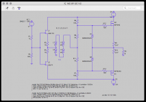
btw. did you put second schematic , framed , on the wall ?
Finally after 3 months with the schematic laying on the table, regular looking at it, I understand the finesse of the M2


Thanks!
Last edited:
Glad that you finally got it.Finally after 3 months with the schematic laying on the table, regular looking at it, I understand the finesse of the M2 ...

Now you may want to consider the Laterals such as the Allfets used on the F7, eliminate both the optocoupler and LM385 by using 4 x 1N4148 for bias and easier to drive due to lower input capacitances.
To members of the Group Buy
PayPal charges 2.99% + $0.30 in fees for sending money when you fund it with a credit card. If the transfer is international there may be also a difference caused by foreign exchange fees.
Most of the payments I have received so far are a little short. I'll communicate with those members about the difference.
- Home
- Amplifiers
- Pass Labs
- Official M2 schematic