Errr.. does this mean that you are going to consider making V3 pcbs available? 🙂
I sure am, assuming all tests out OK. 🙂 I sent them out to fab a few days ago. Still not sure if they are going to beat the Chinese Festival deadline or not. I'm haivng them sent regular mail this time to see how that works out, so will probably add a couple of weeks.
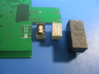
Below is what went out. I found a better relay, a TE Connectivity IM26TS (Mouser 655-IM26TS, Digikey PB1170-ND). Smaller in all dimensions than the Omron G6A I posted above. Most importantly the coil is ultrasensitive with only 4mA draw at 12Vdc, vs. 16mA for the Omron. That relay had been the hangup. 16mA would not have been very battery friendly. I had some email exchange with Omron about using a 24Vdc coil at 12Vdc, but as expected "not advised" due to manufacturing tolerances, even though the couple I have here worked OK. The IM26TS solves the problem. The contacts are still rated at 2A.
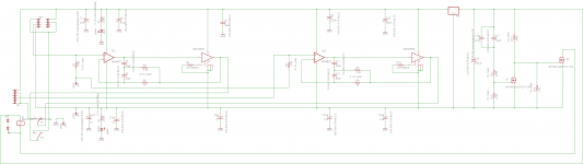
I've put dual parallel capacitor pads for the timing capacitor for the relay on the V3 board. With a 10uF MLCC 1206 capacitor you will get around 8 seconds of turn-on delay. But with another one of the 47uF tantalums instead it will delay almost 45 seconds. I'm using a 78L12 100mA voltage regulator across the combined power rails (24Vdc down to 14Vdc on batteries), an addition over the headphone relay circuit I posted in the O2 modification thread a couple of years ago. Using the voltage regulator the relay turn-on delay time remains constant whether the O2 is on AC or batteries and always keeps the relay coil in its happy zone. I have a combined diode + zener for reverse EMF protection across the relay coil, vs. just the diode, for minimum "off" switching time. I see on the relay data sheet they actually de-rate the opening time slightly if someone goofs and just uses a diode alone for protection. For info, scroll down to the table at the bottom of this PDF:
http://www.google.com/url?sa=t&rct=j&q=&esrc=s&source=web&cd=2&ved=0CC8QFjAB&url=http%3A%2F%2Fwww.te.com%2Fcommerce%2FDocumentDelivery%2FDDEController%3FAction%3Dsrchrtrv%26DocNm%3D13C3311_AppNote%26DocType%3DCS%26DocLang%3DEN&ei=REXfUor1E4nOsAS1rYCIDQ&usg=AFQjCNFh9HS5tLUuL8CFri4nlwb6sksRlg&bvm=bv.59568121,d.cWc&cad=rja
And some good news I've been meaning to post. It looks like I've over-reacted on the voltage magnitude of those O2 turn-on and turn-off thumps being a problem. My fairly sensitive (115dB/V) AKG-K550s (40mV normal volume level) are rated at a maximum of 200mW. That translates to 2.5V, which is 12 times that 200mV turn-on/turn-off thump. Not likely to be a problem of any kind. Only some extremely sensitive IEMs might have an issue. I also remember the issue coming up on RocketScientist / NwAvGuy's comments on his blog site at one point. He shot the issue down for the same reason, as I recall.
So I'm going to go ahead and sell these existing O2 booster boards at cost. 🙂 I'll put the "order" spreadsheet back up at the Goolge Drive link and give the folks on there who expressed interest first dibs, and I'll send out PMs. If not claimed by this Friday I'll open up the remainder to anyone who wants one. Keep an eye on my vendor thread here for details:
http://www.diyaudio.com/forums/vendors-bazaar/237226-parallel-njm4556al-two-stage-amp.html
Cost on the board was around $7 and cost on the board connection pins from Digikey was around $3, plus postage. I'm not going to try to supply components, just the board and pins. Too easy to zap an IC or lose a SMD resistor in the rug during the build (I speak from experience on that one) and need replacements.
One benefit of this existing V2 over the upcoming V3 is the holes for the upside down 1/4" jack (fits if using the taller B3-080 case). I've had to remove those on the V3 boards to fit in the relay circuitry. I did discover a glitch with the optional power management latch circuit I added to these V2 boards. The circuit has to be wired in before the mosfets to work, but on the board I screwed up and have it hooked in after. So those optional parts have to be left unpopulated.
The existing V2 board sounds just fantastic, IMHO. 😀 I listened to one with the OPA827+LME49600 combination in an O2 amp for 4 hours yesterday (on batteries the whole time, too, with the beyer DT-770 cans) while doing some computer work.
Attachments
Last edited:
Could I go on the list too? 🙂
You are added! 🙂 I've just posted a revised order interest spreadsheet at the Google Drive link.
I finally made it to the post office today for a shipping quote. The boards are now ready to ship. I've just posted the details on my vendor thread here:
http://www.diyaudio.com/forums/vend...llel-njm4556al-two-stage-amp.html#post3789288
No commitments of any kind for those folks on the order interest list. If still interested please PM me with your address by next Wednesday the 29th and I'll send you the paypal email address. I can send the boards out immediately once the payment is received. There are 14 boards up for grabs total. 4 more spots on the list are open, plus any from folks on the list now who don't want them.
All boards are priced at-cost here for the DIY effort.
Have fun with the build, and please do post any completed photos and listening results! 🙂
Last edited:
Gerber files now posted for O2 booster board V2.0
I've just posted the Gerber files for V2.0 of this O2 headamp booster board project at the Google Drive link. Anyone interested can submit the Gerbers to their favorite PC board fabrication house (4 layer board) and have their own boards fabricated:
https://drive.google.com/folderview?id=0B67cJELZW-i8Vmp5MDVLNzJxTGc&usp=sharing
Go to the 11_15_2013 V2.0 folder, then the Gerber file folder. I also have a PDF in there with instructions for submitting the Gerber file to Seeed Studio (the outfit I've been using) to fabricate boards. They are located here:
Seeed Studio Bazaar,Boost ideas,extend the reach - Fusion PCB
I haven't used OSH park, but the instructions should be similar. With Seeed Studio the minimum quantity is 5 boards, then they also have 10, 20, 50, or 100 board options. The cost per board goes down at higher quantities, of course.
I've removed the 4 power management latch circuit components entirely in this Gerber file. Everything else is the same, except for some minor text label adjustments.
Last edited:
Updated BOM posted
I've just posted an updated BOM for V2.0 of this O2 booster board project at the Google Drive link. It is the same as previous, but with these changes:
I've adopted a good suggestion and split the various optional O2 modifications up into their own tables: LED, 1/4" jack, and the now-defunct power management latch circuit. Makes it easier to see which parts go with which O2 modifications.
Mouser is out of stock now on the LEDs, but they show an arrival date for new stock in just a week on 2/3/2014. Digikey has a large stock of those LEDs right now. The LEDs also come in different colors and other colors are in stock at Mouser.
I've changed the vendor on the 3.3k resistors in the BOM to panasonic just because both Mouser and Digikey stock that same part. No changes to the resistor specification itself.
The pads on the board for the 10uF capacitors are sized for 1210 size SMD, which matches up with a 50V rating. I've since decided that 50V is overkill. 35V 1206 sized 10uF X7R MLCC parts also fit just fine on those SMD pads and cost about $0.40 less.
Last edited:
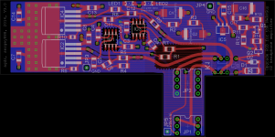
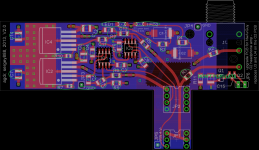
Booster board component identification diagram & R7/R10
I've put together the marked-up layout diagram below that helps show which text part labels go with which parts on the O2 booster board, especially in the middle where the parts are close together. The PDF file is the same thing as the PNG, just can be magnified a lot larger in the PDF viewer if needed.
It occured to me last night that it wouldn't be particularly clear which parts some of the labels were associated with, like R8 or R6, if someone hadn't been the one to layout the board. 🙂
I've also posted these pictures at the project's Google Drive link.
I also have realized there was no mention of R7 and R10 in the BOM. Fixed. Those are more optional modifications. Leaving those resistors out sets the LME49600 bandwidth at 110mHz (I recommend to leave it this way), while soldering in the 100R 0805-sized (smaller than the rest of the resistors and capacitors, harder to solder) SMD resistors I've added to the BOM will increase the BW to 180mHz - and double the idle current from 7mA to 13mA. 110mHz is more than adequate for audio. The higher BW setting shows a miniscule noise floor improvement in the datasheet, not likely audible and not worth the extra current draw. But... if someone is running their O2 mainly as a AC-powered desktop and really wants to give it a try, the pads are there so go right ahead. 🙂 Best to solder those resistors in before soldering the LME49600s. Soldering them in after mounting the LME49600s would be harder to do.
Attachments
Last edited:
First post in this thread updated with latest file locations
I've just updated the top of the very first post in this thread with an index to which board versions match up with which file folders at the Google Drive link.
I've decided that rather than release Gerber files for the V2.0 boards with the power management circuit error (the ones now shipping at the vendor thread), I've removed those 4 components to correct the error on a new V2.1. V2.1 is in a new 1_26_2014 folder.
So those building up their V2.0 board I've shipped should still use the files in the 11_15_2013 folder for their build. Anyone sending the V2.1 Gerber files in the 1_26_2014 folder out for PC board fabrication should use the files in that folder for their build. The V2.1 board is exactly the same as V2.0 but with the PM latch parts removed, a few minor revisions of the text labels for clarity, and pads added for a through-hole 10K 1/8W resistor to be added between the power rails for more anti-turnoff thump reduction. The board's LEDs still keep the drain-down rail voltage about 2.1Vdc above ground, same s the O2's op amps. The new 10K resistor allows the rails to drain linearly all the way to 0Vdc quickly upon O2 mosfet turn-off. That same resistor can easily be added to the V2.0 board by soldering between pins 4 of JP2 (lower left corner) and pin 6 of JP1 (upper right corner).
The files for the new V3.0 with the headphone relay, which is being fabricated, will be in the 1_18_2014 folder.
After tomorrow 1/29/2014 I'll assume that everyone on the "orders" interest list in the 11_15_2014 folder who wants a board has contacted me, and I'll make the remaining boards available to anyone. I've updated the list with ship dates.
Please feel free to PM me with build questions, documentation questions, suggestions, and do feel free to post your build pictures and results here! 🙂
Last edited:
V3.0 boards work
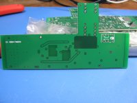
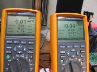
I just received the V3.0 boards for this O2 headphone amplifier booster board project and built one up. It works! 😀
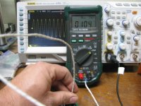
The new headphone relay works perfectly. From the DMM peak-reading pictures below (second post, ran out of picture posting space), upon O2 turn-on there is now exactly zero turn-on transient voltage or thump. Just the DC offset which is reading 25uV for one channel and 50uV for the other (I built this one with OPA140 chips). On turn-off, from the photos, the turn-off transient is now down to around 15mV, down from the 200mV the O2 produces in stock form. Still slightly audible but a 90% improvement over the basic O2 headamp. No worries at all about any headphone or IEM damage from thumps at this low level.
On the ODA amplifer I was able to use a second set of contacts in the on/off switch to loop the relay coil through, resulting in zero turn-off thump on that one in addition to the zero turn-on thump. Couldn't do that here since RocketScientist is using all his switch contacts, but a 90% reduction is more than adequate.
I have updated materials for the V3.0 boards posted at the Google Drive link now, under the 1_18_2014 V3.0 folder. BOM, updated build instructions, circuit, layout, photos, and part ID diagram. I should have the Gerber files (to make your own boards) posted later today.
I ordered 10 boards this time and will probably have a few extras for sale at cost if anyone should be interested. Keep an eye on my vendor forum thread. 🙂
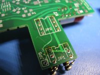
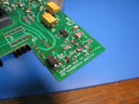
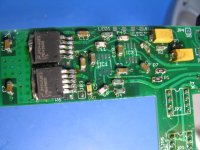
Photos:
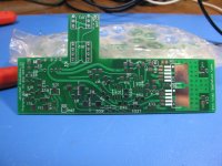
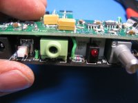
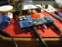
* first two are the front and back of V3.0.
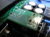
* next two show the size comparison between the TE connectivity relay I used, vs. the Omron G6A I posted about above. Much smaller! The second photo shows a good way to solder. Solder one pin first, then put your thumb on it and resolder while pressing up to get the relay flush. Then solder the rest of the pins.
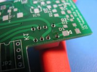
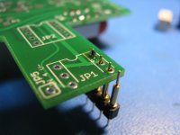
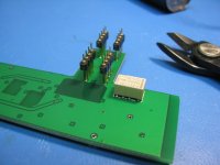
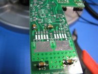
* the next four show a better way of soldering the board connection pins. Just solder one pin on each 4-pin strip, so the strip can be bent left and right as needed to line up with U3 and U4 on the O2 board. Note that the plastic strip on the connection pins goes down, toward the O2 PC board. Then slide the sandwhich into the O2 case, pulling the top up slightly if needed, to get the boards aligned. THEN solder the rest of the connection pins. The final photo shows how closely the connection pin plastic should sit to the U3 and U4 sockets. If it doesn't then one of your pins strips isn't in the U3 / U4 socket holes properly.
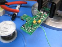
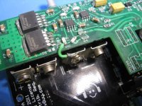
* then remove the booster board from the O2 again. The next photo shows the way the relay and the 4 sets of connection pins should look, under the board, when finished.
* the final photo shows how C8 should be soldered on first due to the close proximity to the buffer chips. This is in the build instructions.
I just received the V3.0 boards for this O2 headphone amplifier booster board project and built one up. It works! 😀
The new headphone relay works perfectly. From the DMM peak-reading pictures below (second post, ran out of picture posting space), upon O2 turn-on there is now exactly zero turn-on transient voltage or thump. Just the DC offset which is reading 25uV for one channel and 50uV for the other (I built this one with OPA140 chips). On turn-off, from the photos, the turn-off transient is now down to around 15mV, down from the 200mV the O2 produces in stock form. Still slightly audible but a 90% improvement over the basic O2 headamp. No worries at all about any headphone or IEM damage from thumps at this low level.
On the ODA amplifer I was able to use a second set of contacts in the on/off switch to loop the relay coil through, resulting in zero turn-off thump on that one in addition to the zero turn-on thump. Couldn't do that here since RocketScientist is using all his switch contacts, but a 90% reduction is more than adequate.
I have updated materials for the V3.0 boards posted at the Google Drive link now, under the 1_18_2014 V3.0 folder. BOM, updated build instructions, circuit, layout, photos, and part ID diagram. I should have the Gerber files (to make your own boards) posted later today.
I ordered 10 boards this time and will probably have a few extras for sale at cost if anyone should be interested. Keep an eye on my vendor forum thread. 🙂
Photos:
* first two are the front and back of V3.0.
* next two show the size comparison between the TE connectivity relay I used, vs. the Omron G6A I posted about above. Much smaller! The second photo shows a good way to solder. Solder one pin first, then put your thumb on it and resolder while pressing up to get the relay flush. Then solder the rest of the pins.
* the next four show a better way of soldering the board connection pins. Just solder one pin on each 4-pin strip, so the strip can be bent left and right as needed to line up with U3 and U4 on the O2 board. Note that the plastic strip on the connection pins goes down, toward the O2 PC board. Then slide the sandwhich into the O2 case, pulling the top up slightly if needed, to get the boards aligned. THEN solder the rest of the connection pins. The final photo shows how closely the connection pin plastic should sit to the U3 and U4 sockets. If it doesn't then one of your pins strips isn't in the U3 / U4 socket holes properly.
* then remove the booster board from the O2 again. The next photo shows the way the relay and the 4 sets of connection pins should look, under the board, when finished.
* the final photo shows how C8 should be soldered on first due to the close proximity to the buffer chips. This is in the build instructions.
Attachments
-
 IMG_2272.JPG140.9 KB · Views: 235
 -
 IMG_2271.JPG184.4 KB · Views: 239
 -
 IMG_2273.JPG163.8 KB · Views: 137
 -
 IMG_2274.JPG135.5 KB · Views: 126
 -
 IMG_2275.JPG124.8 KB · Views: 116
 -
 IMG_2277.JPG153.4 KB · Views: 115
 -
 IMG_2279.JPG150.1 KB · Views: 116
 -
 IMG_2278.JPG139 KB · Views: 120
 -
 IMG_2282.JPG133.3 KB · Views: 126
 -
 IMG_2283.JPG168.6 KB · Views: 139
Last edited:
booster board V3.0 photos, continued...
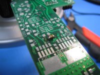
* the first photo shows that while soldering in C8 first, you may want to just go ahead and solder all 4 of the 10uF 35V caps in, which you have that bag from Mouser out.
* the next photo shows everything soldered on but IC1 and IC3, the LEDs, and the relay circuitry. The build instructions say to solder in IC1 and IC3 last to help reduce the change of static damage. Note that I haven't used de-fluxing cleaner yet.
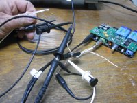
* the next photo shows all the relay circutry soldered on the other end of the board.
* the next three photos shows the two ground wires being soldered on and connected to the O2 PC board. O2 booster board V3.0 uses two ground wires, as explained in the build instructions. The short one goes to either middle battery terminal. The long one goes to the grounded side of the 40.2K resistors on the O2 PC board, as the second photo shows. The wire goes around the back of the O2's output jack.
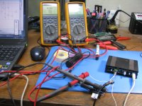
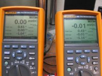
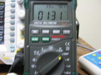
* the next photo shows the test setup for checking turn-on and turn-off transients. The DMMs are set to a fast-responding DC peak voltage hold mV scale. One DMM on the output of each channel with test headphones attached.
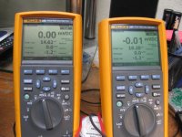
* the next two photos show the peak mV dc readings before (first photo) and after (second photo) the headphone relay closes. Essentially a non-event. 🙂 The final photo shows the captured peak readings on O2 amp switch-off. Around 15mV, down from 200mV for the original O2 amp. Note the measured DC output offset on the second DMM photo at the top of the display - 10uV and 40uV! Can't beat that. I'm using the OPA140 chips in this build.
* the first photo shows that while soldering in C8 first, you may want to just go ahead and solder all 4 of the 10uF 35V caps in, which you have that bag from Mouser out.
* the next photo shows everything soldered on but IC1 and IC3, the LEDs, and the relay circuitry. The build instructions say to solder in IC1 and IC3 last to help reduce the change of static damage. Note that I haven't used de-fluxing cleaner yet.
* the next photo shows all the relay circutry soldered on the other end of the board.
* the next three photos shows the two ground wires being soldered on and connected to the O2 PC board. O2 booster board V3.0 uses two ground wires, as explained in the build instructions. The short one goes to either middle battery terminal. The long one goes to the grounded side of the 40.2K resistors on the O2 PC board, as the second photo shows. The wire goes around the back of the O2's output jack.
* the next photo shows the test setup for checking turn-on and turn-off transients. The DMMs are set to a fast-responding DC peak voltage hold mV scale. One DMM on the output of each channel with test headphones attached.
* the next two photos show the peak mV dc readings before (first photo) and after (second photo) the headphone relay closes. Essentially a non-event. 🙂 The final photo shows the captured peak readings on O2 amp switch-off. Around 15mV, down from 200mV for the original O2 amp. Note the measured DC output offset on the second DMM photo at the top of the display - 10uV and 40uV! Can't beat that. I'm using the OPA140 chips in this build.
Attachments
-
 IMG_2289.JPG160.7 KB · Views: 131
 -
 IMG_2288.JPG186.9 KB · Views: 137
 -
 IMG_2284.JPG154.5 KB · Views: 130
 -
 IMG_2291.JPG154.5 KB · Views: 120
 -
 IMG_2293.JPG151.8 KB · Views: 129
 -
 IMG_2294.JPG210.9 KB · Views: 156
 -
 IMG_2297.JPG215.5 KB · Views: 126
 -
 IMG_2301.JPG186.3 KB · Views: 98
 -
 IMG_2300.JPG179 KB · Views: 103
 -
 IMG_2299.JPG170.6 KB · Views: 117
Last edited:
Here more pictures of V3.0 testing.
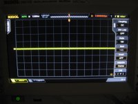
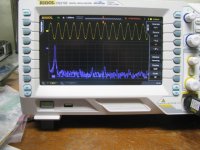
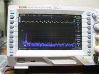
The first is scope shot to show no oscillation with capacitive loading. That is a 0.01uF axial cap in the clips and a 5nS time base on the scope. I've also tried 1000pF and 500pF with a few different headphone loads. I've upgraded the scope here to one that has a measured 175mHz 3dB point, so the bandwidth now covers that 80mHz peak in the LME49600 that Sergey888 found. I noticed that National does have mention of that buried in the datasheet graphs.
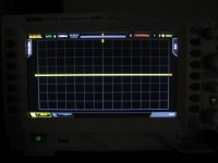
The second scope shot with a 5mS time base shows no 60Hz or the next few harmonics. I wanted to verify that given the position of the relay now vs. the AC input parts in the O2. Both scope shots were taken with the O2 on AC power with a 16Vac adapter. O2 input disconnected (grounded).
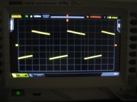
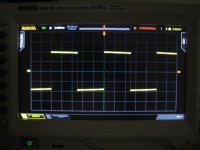
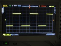
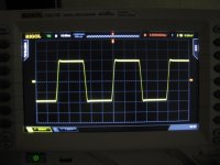
The square wave shots are at 20kHz, 1kHz, 100Hz, and 20Hz. Remember that the droop on the very low frequency wave is due to the O2's coupling capacitor in the middle.
The first is scope shot to show no oscillation with capacitive loading. That is a 0.01uF axial cap in the clips and a 5nS time base on the scope. I've also tried 1000pF and 500pF with a few different headphone loads. I've upgraded the scope here to one that has a measured 175mHz 3dB point, so the bandwidth now covers that 80mHz peak in the LME49600 that Sergey888 found. I noticed that National does have mention of that buried in the datasheet graphs.
The second scope shot with a 5mS time base shows no 60Hz or the next few harmonics. I wanted to verify that given the position of the relay now vs. the AC input parts in the O2. Both scope shots were taken with the O2 on AC power with a 16Vac adapter. O2 input disconnected (grounded).
The square wave shots are at 20kHz, 1kHz, 100Hz, and 20Hz. Remember that the droop on the very low frequency wave is due to the O2's coupling capacitor in the middle.
Attachments
Last edited:
V2 installed and working 😀
Assembly was pretty straight forward, though i did run into an issue on a prebuilt O2 (i have two) in that the two power supply caps C8/C9, and the two output caps C13/C14 weren't sitting flush against the PCB so they needed pushed home to make room for the booster PCB. Once i confirmed everything was working without magic smoke coming out i installed it into my main amp. I should also note its important to get the two LME49600 buffers soldered as close to the PCB as possible as there is zero clearance with the case.
I chose the OPA827 opamps as it seemed a worthwhile upgrade for the cost vs performance. I also installed the two LED's, just because. As for DC offset, i measured .003v on the left/right channel as stock, and nothing after as my meter isn't sensitive enough.
So how does it sound? Surprising, very surprising. I confess i havent used the O2 in a long time as i've moved onto building valve amps with capacitors that cost more than the O2, but yet i'm still stunned by how good this sounds. As i have two O2's i was able to do some side by side comparisons and the stock one is pretty much as i remember, clean, precise, maybe a little bit too clinical, and lacking a bit of presence and low end energy. The booster modded version however is a different story, it somehow manages not to sound like an opamp, it has a soul and sucks you in to the music. I'm going to have to spend more time with it to rationalize the difference, but what i hear so far i like, a lot.
Nice work Agdr
Attachments
V3.0 maximum load testing
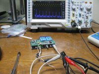
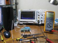
Here is a fun maximum load test on the V3.0 O2 booster board. I'm using an 8 ohm speaker here since I wouldn't be able to push this much power into most headphones.
The first photo shows the test setup. I have an 8 ohm speaker connected to the booster board. The first batch of testing is done on batteries since the O2's un-heatsinked voltage regulators would overheat with the load. That is a thermocouple hooked to the green meter. I did a test using the O2 amp on AC and stopped when NwAvGuy's regulator tabs hit 180 degrees F.
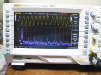
The setup is being fed from a function generator set to make sine waves. The scope is set for split screen, with FFT on the bottom and the actual waveform on the top.
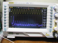
The next two photos show the spectrum out of the generator, for reference, with it hooked to the (10K) input of the O2. The generator is set for just under 1 volt peak, while the O2 is set up for 2.5X gain. The first photo is the spectrum using square waves, while the second is the 1kHz sinusoid used in the tests. The vertical scale is in dB so the fuzz at the bottom is way down, just a few mV. Keep in mind that scope FFTs are much noiser than audio software + soundcard or AP/dScope readings. That noise isn't the generator as much as the scope and the pickup noise in the leads. I also have the scope set for input averaging to smooth out the FFT, and I'm using a Hanning window.
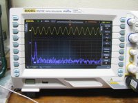
The next photo shows the FFT with the output of the booster board into the speaker just below clipping at 2.2Vpeak. The next photo is at 2.4Vpeak showing the onset of clipping, which clearly shows up in the FFT with all those harmonics popping up. You can see a bit of distortion showing up at the bottom peaks of the waveform at the top of the screen.
With the booster board output pushing the 2.2Vpeak into the 8ohm speaker (before clipping), the next photo shows the temperature rise on the LME49600 chips is just 104 degrees F. Easily sustainable long term for both the chip and the board foil.
I've measured the speaker's actual impedance at 1kHz to be closer to 10 ohms, so for accuracy I'm using 10R in the calculations. The power into the speaker is sqr[(2.2Vac)(0.707)] / 10 = 242mW. More than the vast majority of headphone require, so this already proves the booster board can tackle high current (low impedance + low sensitivity) headphones with ease. The rms current through the LME49600 chips is (2.2)(0.797)Vac / 10 = 155mA. Well within specifications for the 250mA - rated LME49600.
To ratchet things up a notch, in the next photo I have +/-11.9Vdc from an external tracking supply fed into the O2 to get around the problem of its voltage regulators overheating with the large loads. The next two photos shows the waveform and FFT into the speaker just before (3.2Vac peak now) and just after clipping. Again the onset of clipping is obvious from that array of harmonics that get generated. The test signal is still 1kHz. So the final photo (sorry about hte blur!) shows that the LME49600 temperature is now up to 131 degrees F, and stable at that level in open air. That would still be perfectly fine from the chip's standpoint, but the OC board foil may not be able to take that long term without de-bonding. Inside the closed case that temp would likely increase considerably. This level of loading is pretty much an absolute maximum for the booster board.
So just before clipping the power into the speaker is now sqr[(3.2Vac)(0.707)] / 10 = 512mW! The rms current through the LME49600 is now [(3.2Vac)(0.707)] / 10 = 226mA, just barely under the LME49600's 250mA rating. Peak current is 3.2Vac / 10 = 320mA.
All in all I'm quite happy with the O2 booster board's results! 😀
Here is a fun maximum load test on the V3.0 O2 booster board. I'm using an 8 ohm speaker here since I wouldn't be able to push this much power into most headphones.
The first photo shows the test setup. I have an 8 ohm speaker connected to the booster board. The first batch of testing is done on batteries since the O2's un-heatsinked voltage regulators would overheat with the load. That is a thermocouple hooked to the green meter. I did a test using the O2 amp on AC and stopped when NwAvGuy's regulator tabs hit 180 degrees F.
The setup is being fed from a function generator set to make sine waves. The scope is set for split screen, with FFT on the bottom and the actual waveform on the top.
The next two photos show the spectrum out of the generator, for reference, with it hooked to the (10K) input of the O2. The generator is set for just under 1 volt peak, while the O2 is set up for 2.5X gain. The first photo is the spectrum using square waves, while the second is the 1kHz sinusoid used in the tests. The vertical scale is in dB so the fuzz at the bottom is way down, just a few mV. Keep in mind that scope FFTs are much noiser than audio software + soundcard or AP/dScope readings. That noise isn't the generator as much as the scope and the pickup noise in the leads. I also have the scope set for input averaging to smooth out the FFT, and I'm using a Hanning window.
The next photo shows the FFT with the output of the booster board into the speaker just below clipping at 2.2Vpeak. The next photo is at 2.4Vpeak showing the onset of clipping, which clearly shows up in the FFT with all those harmonics popping up. You can see a bit of distortion showing up at the bottom peaks of the waveform at the top of the screen.
With the booster board output pushing the 2.2Vpeak into the 8ohm speaker (before clipping), the next photo shows the temperature rise on the LME49600 chips is just 104 degrees F. Easily sustainable long term for both the chip and the board foil.
I've measured the speaker's actual impedance at 1kHz to be closer to 10 ohms, so for accuracy I'm using 10R in the calculations. The power into the speaker is sqr[(2.2Vac)(0.707)] / 10 = 242mW. More than the vast majority of headphone require, so this already proves the booster board can tackle high current (low impedance + low sensitivity) headphones with ease. The rms current through the LME49600 chips is (2.2)(0.797)Vac / 10 = 155mA. Well within specifications for the 250mA - rated LME49600.
To ratchet things up a notch, in the next photo I have +/-11.9Vdc from an external tracking supply fed into the O2 to get around the problem of its voltage regulators overheating with the large loads. The next two photos shows the waveform and FFT into the speaker just before (3.2Vac peak now) and just after clipping. Again the onset of clipping is obvious from that array of harmonics that get generated. The test signal is still 1kHz. So the final photo (sorry about hte blur!) shows that the LME49600 temperature is now up to 131 degrees F, and stable at that level in open air. That would still be perfectly fine from the chip's standpoint, but the OC board foil may not be able to take that long term without de-bonding. Inside the closed case that temp would likely increase considerably. This level of loading is pretty much an absolute maximum for the booster board.
So just before clipping the power into the speaker is now sqr[(3.2Vac)(0.707)] / 10 = 512mW! The rms current through the LME49600 is now [(3.2Vac)(0.707)] / 10 = 226mA, just barely under the LME49600's 250mA rating. Peak current is 3.2Vac / 10 = 320mA.
All in all I'm quite happy with the O2 booster board's results! 😀
Attachments
-
 IMG_2340.JPG132 KB · Views: 107
 -
 IMG_2338.JPG169.6 KB · Views: 117
 -
 IMG_2336.JPG174.2 KB · Views: 115
 -
 IMG_2334.JPG206.6 KB · Views: 117
 -
 IMG_2327.JPG170 KB · Views: 119
 -
 IMG_2325.JPG171.9 KB · Views: 117
 -
 IMG_2324.JPG170.3 KB · Views: 121
 -
 IMG_2319.JPG156.8 KB · Views: 117
 -
 IMG_2318.JPG210.8 KB · Views: 130
 -
 IMG_2323.JPG198.4 KB · Views: 156
Last edited:
V2 installed and working 😀
Hey thank you for the feedback! I'm actually just now reading your post. From the time stamp you must have posted just before I did last night and I never thought to scroll up when I was done.😛
Good point about those 4 O2 capacitors needing to be flush. I'll add that to the build instructions. The clearance to those caps is close enough I carved that square section of bottom foil out of the board where it sits over the top of C8 and C9, just to make sure nothing connected accidentally.
Very true about the LME49600s needing to be down flat. I've found it makes a huge difference in soldering those to use a wide chisel tip on the iron vs. the regular narrow tip. On this latest build just for fun I tried soldering in the LME49600s with the regular tip and just couldn't do it. Only a small area of solder area would melt. Then I switched over to a 3/16" wide chisel tip - same 80W soldering station - and no troubles at all. The whole surface area melted just fine. I guess it is an issue of getting enough heat to transfer from the tip to the part.
I've found that a two-step soldering process works well with the LME49600. After getting the part soldered up the first time and the 5 leads aligned, I go back and while pressing on the top of the part with a tool, I re-heat the tab & foil to get it down flat on the board. On this last build when I did that one of the chips dropped a noticable amount, like 1/32" or so.
I have the front panel hole measurements for those LEDs in the build instructions now.
Thanks for the listening report! 🙂 I'll be quite curious to hear what people's experiences are using various headphones.
Last edited:
No problem. Just to confirm on the caps, my prebuilt O2 had the regular Nichicon and Kemet caps, and the one i built has the Panasonic FM and Wima caps which are listed in the BOM as optional parts, booster fitted both amps without issue.
The 49600's were a challenge alright, i ended up creating a pool of solder with the tip inside to maximize the heat transfer into the board/chip while pressing them down with tweezers. I was worried i had cooked them they got so hot.
I've been listening so far with Ms-Pros (variation of Grado RS1), but i'll try the HD650's and see how it handles a high impedance load. The O2 and HD650 was always a bit weak sounding to me so will be interesting to see.
The power on/off noise is different alright, its more of a sharp sput sound rather than the soft thump of the stock config but its a non issue in my opinion.
No problem. Just to confirm on the caps, my prebuilt O2 had the regular Nichicon and Kemet caps, and the one i built has the Panasonic FM and Wima caps which are listed in the BOM as optional parts, booster fitted both amps without issue.
Good point about cap substitutions. In fact one of the O2 mods I posted in that mod thread was increasing the 2.2uF's to 4.7uF WIMAs. I think that 4.7's were the same height but I should check to make sure.
I've just updated the V2.0 and V3.0 build instructions at the Google Drive link with this issue and the LME49600's flatness. Thanks again for the feedback. 🙂
I've also updated the first posting in this thread to reflect the V3.0 boards being fabricated.
Last edited:
Remember to cut the leg off the gain switch on the O2
It sounds like a few people are building up brand new O2 boards for the first time along with their O2 booster board. With your O2 build, remember that NwAvGuy has one layout error on there that needs a quick fix. He posted about this in the O2 thread but the post is burried in that huge thread now.
One corner leg of the gain switch sits right above a through-hole on the O2's PC board. If they touch the gain on the left channel will go super-high, essentially turning it into a comparator as the signal clips against both power rails, and it will turn your input signal into square waves. Those will go right through the coupling capacitor in the O2, being AC, and make it to the headphones.
The fix is to clip that particular leg of the O2's gain switch off with wire cutters before soldering it in. You can bend it up enough with the tip of a screwdriver to clear the through-hole if the switch is already installed.
I've just added mention of this issue to the V2 and V3 O2 booster board build instructions.
Last edited:
The first pic is a 10k resister across +15v and -15v like the version 3 board.
The second and third is a clean way to ground the booster board.
Just some ideas. First time posting pics on this forum. 🙂
The second and third is a clean way to ground the booster board.
Just some ideas. First time posting pics on this forum. 🙂
An externally hosted image should be here but it was not working when we last tested it.
An externally hosted image should be here but it was not working when we last tested it.
An externally hosted image should be here but it was not working when we last tested it.


- Home
- Amplifiers
- Headphone Systems
- O2 headamp output booster PCB