Id also like to find an opamp for the gain stage with lower power consumption. The njm2068 is listed at 5-8ma and the Lme49720 I am using is listed at 10-12ma but neither datasheet says if that is per amplifier or per chip? Anyone know?
The datasheets are so vauge about that (per amp or per chip) it probably be necessary to actually measure it. Not clear to me either! The OPA2140 is the one chip I'm aware of that has substantialy less idle current at 2mA per section. The data sheet on the 140/240 actually does state "per amplifier".
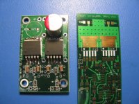
Good O2 Booster Board testing comments from JDS Labs
Hey I just spotted some testing comments that John at JDS Labs posted for the booster board over at Head-FI, here:
O2 AMP + ODAC - Page 204
Here are some thoughts from my end. 🙂 I really appreciate the testing effort on John's part! A lot of time goes into it. A big thanks goes out to John. 🙂
* A couple of weeks ago I added a restriction in the build instructions that the +/-15Vdc modification should only be used with 300R and up headphones for exactly the reason John mentions. There isn't enough heat sink foil around the LME49600 chips on the booster board (and the bottom via the thermal vias) to support anything lower than 300R at +/-15Vdc. An associated issue is the lack of heat-sinking on the O2's voltage regulators. +/-15Vdc power rails would require a 16Vac transformer. Anything lower than a 300R load would pull enough current through the O2's voltage regulators to cause them to go into thermal shutdown. The +/-15Vdc modification would work with headphone impedances lower than 300R if the volume level (maximum output swing) is restricted, but as John mentions something like that can't be shipped in production. All levels of the volume control have to work. So that is why the 300R and up restriction at +/-15Vdc. For headphones that need it, at 300R and above, +/-15Vdc would give about 3V of extra swing.
* With the +/-12Vdc O2 rails *and a 12Vac transformer*, I'll have to have another chat with John to make sure I understand the test conditions he is using. We've exchanged some PMs and by 35% stronger I think that may mean 7Vrms out instead of the 4.25Vrms maximum that NwAvGuy shows in the "THD+N vs,. Output and Max Power on AC" plot in his blog writeup here:
O2 AMP + ODAC - Page 204
An interesting discovery popped out from John's testing. That chart in NwAvGuy's writeup has left off an important test condition. Those maximum power levels ONLY apply when using the 12Vac transformer, but at 12Vac and the maximum output currents the O2's voltage regulators are likely in dropout and not doing anything to reduce line ripple. Going up to a 16Vac transformer would put 4 more volts across the O'2 voltage regulators that they can't tolerate. When using a 16Vac transfomer with the O2' his maximum power levels in that chart would have to be reduced by about 4V to keep the O2's voltage regulator dissipation the same. But the voltage regulators in the O2 amp would not be in dropout and doing something for ripple reduction.
Back to the booster board, what may be going on here is the O2's original NJM4556A chips current limit at about 100mA, which results in that 4V maximum output at 32R. The booster board chips don't current limit until 250mA. I may very well need to list the maximum output swing at 3V or lower at 32R. I will look into that more this weekend. I tested the booster chips at 250mA in one set of thread posts, using an external power supply, to make sure they could burst up to 250mA on musical peaks. But I was relying on the math for the continuous average load power dissipation numbers. Thanks again to John for the testing here!
* It does look like the THD+N may be limited by the NJM2068 chip, which is an interesting discovery! If I'm looking at his dScope plots correctly the booster was just slightly lower in THD+N than the stock O2 with the NJM2068 chip in place, really within the margin of error, which makes it a wash. I've also sent John one of the dual LME49990 adaptors to try in place of the NJM2068, if he wants to give that a try with the dScope, which may produce lower THD+N numbers that would make it through the booster. They also may make it through the NJM4556As too - that would be another very interesting dScope test (dual LME49990 in place of NJM2068 and the original NJM4556A's). NwAvGuy had posted in his blog that the NJM4556A were the limiting factor on THD+N, and I believed the same from the data sheets, but it may not be the case. That does say something good for the NJM455As, and hopefully for the ODA which uses those same chips in the output stage, just more of them and SIP packages.
I've just mailed out a booster board with OPA827 chips to John also (the booster he has been testing has the OPA140 chips). If theOAP140 version doesn't produce significantly lower THD+N with a dual LME49990 adaptor in for the NJM2068 chip at less-than-maximum output levels, maybe the OPA827 version will. The OPA827s shows lower THD+N on the datasheet at any rate.
* And in addition to the relay the booster provides that lower DC output offset. Lower offset isn't likely to make a difference for the majority of headphones, but may for some more sensitive IEMs.
A big thanks goes out to John at JDS Labs!! 🙂
Last edited:
For now, 89dB/mW minimum headphone sensitivity at 32 ohms
To address the JDS Labs test results in the post above about booster board power dissipation at 32R load, until I can get time to run some tests this weekend and next week I'm going to say limit the minimum sensitivity of 32 ohm headphones you use with the O2 booster board to 89dB/mW.
From the spreadsheet posted here at the project's Google Drive link:
https://drive.google.com/folderview?id=0B67cJELZW-i8S0tvT25veW41eVU&usp=sharing
89dB/mW sensitivity headphones at 32R requires 2Vrms to reach 110dB sound pressure level. Again, nobody should be listening to headphones at 110dB continuous (see the hearing damage level chart at the bottom of that spreadsheet) but it does show that sound peaks can go that high. 89dB/mW and above should still cover a lot of (32R) headphones. For 32R headphones with lower sensitivity than that, or for peaks higher than 110dB/mW, you need an ODA or other amp like AMB's b22 that can supply additional current with the output chip dissipation ability (and voltage regulator dissipation) to support it.
By limiting the 32R headphones you use to 89dB/mW sensitivity or higher the headphones would be insanely loud above 2Vrms or so, the levels at which power dissipation would become a problem with the booster board. So as always, turn your volume control all the way down when plugging in a new set of headphons and then adjust the volume level up from there.
It is possible the booster board cmay go higher than 2Vrms into 32, but I need some time to attach thermocouples and re-create the arrangement that John had setup in his testing.
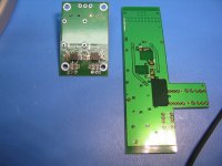
Also below are some interesting comparison photos between the LME49600 foil heatsink area on the O2 Booster Board and the previous version (a couple of years ago) of OPC's "Wire" board using a similar side-by-side arrangement for 2 LME49600s. The booster board has about 25% less foil on the top, but about 2x to 3x more on the bottom with a bunch of thermal vias. I'll have to admit I've never tried cranking a "Wire" board up past 4Vrms into 32R, which it should be able to do from a power supply standpoint since the Wire runs on +/-15Vdc vs. the +/-12Vdc with the standard O2 headamp. Given the foil areas I would suspect the Wire would experience the same thermal overheating above 3 or 4Vrms or so into 32R with 89dB/mW or less sensitivity headphones given the similar foil areas. Anyone with a Wire out there tried it? 🙂
I'm open to suggestions here, too! 🙂 One thing I've already done on the layout is add longer front foil past the front of the LME49600 chips, then added another row of thermal vias to transfer more heat ot he rear foil Might be worth adding thermal vias on the LME49600 pads themselves like OPC has done with his new LPUHP board. That certain did draw the iron heat away well while soldering! If I poinder it long enough there may even be a way to make a thermal connection between that small strip of front foil above the LME49600 tabs and the top of the case with a small block of metal clamped down.
To address the JDS Labs test results in the post above about booster board power dissipation at 32R load, until I can get time to run some tests this weekend and next week I'm going to say limit the minimum sensitivity of 32 ohm headphones you use with the O2 booster board to 89dB/mW.
From the spreadsheet posted here at the project's Google Drive link:
https://drive.google.com/folderview?id=0B67cJELZW-i8S0tvT25veW41eVU&usp=sharing
89dB/mW sensitivity headphones at 32R requires 2Vrms to reach 110dB sound pressure level. Again, nobody should be listening to headphones at 110dB continuous (see the hearing damage level chart at the bottom of that spreadsheet) but it does show that sound peaks can go that high. 89dB/mW and above should still cover a lot of (32R) headphones. For 32R headphones with lower sensitivity than that, or for peaks higher than 110dB/mW, you need an ODA or other amp like AMB's b22 that can supply additional current with the output chip dissipation ability (and voltage regulator dissipation) to support it.
By limiting the 32R headphones you use to 89dB/mW sensitivity or higher the headphones would be insanely loud above 2Vrms or so, the levels at which power dissipation would become a problem with the booster board. So as always, turn your volume control all the way down when plugging in a new set of headphons and then adjust the volume level up from there.
It is possible the booster board cmay go higher than 2Vrms into 32, but I need some time to attach thermocouples and re-create the arrangement that John had setup in his testing.
Also below are some interesting comparison photos between the LME49600 foil heatsink area on the O2 Booster Board and the previous version (a couple of years ago) of OPC's "Wire" board using a similar side-by-side arrangement for 2 LME49600s. The booster board has about 25% less foil on the top, but about 2x to 3x more on the bottom with a bunch of thermal vias. I'll have to admit I've never tried cranking a "Wire" board up past 4Vrms into 32R, which it should be able to do from a power supply standpoint since the Wire runs on +/-15Vdc vs. the +/-12Vdc with the standard O2 headamp. Given the foil areas I would suspect the Wire would experience the same thermal overheating above 3 or 4Vrms or so into 32R with 89dB/mW or less sensitivity headphones given the similar foil areas. Anyone with a Wire out there tried it? 🙂
I'm open to suggestions here, too! 🙂 One thing I've already done on the layout is add longer front foil past the front of the LME49600 chips, then added another row of thermal vias to transfer more heat ot he rear foil Might be worth adding thermal vias on the LME49600 pads themselves like OPC has done with his new LPUHP board. That certain did draw the iron heat away well while soldering! If I poinder it long enough there may even be a way to make a thermal connection between that small strip of front foil above the LME49600 tabs and the top of the case with a small block of metal clamped down.
Attachments
Last edited:
Up to 7Vrms OK into 32R with music but not with sine waves
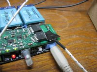
OK, I took off early this afternoon and set up a power dissipation test rig for the O2 Booster Board with 33R loads on each channel. I believe that I've found the problem: music vs. testing with pure sine waves. NwAvGuy himself mentioned this in his blog, that if using pure sine waves the O2 headamp should only be run for 10 minutes or less at full power. The same will apply to the O2 booster board + O2 headamp combination.
In the test setup below I first used music with 4Vpeaks (2.8Vrms), then ran it all the way up to 7V peaks(5Vrms), the maximum before the O2 and the 12Vac power adaptor clip. The result: no thermal power dissipation problems at all with either the booster board or the O2's voltage regulators. I did not try the tests with pure sine waves instead of music. The power dissipation with sine waves would typically be 2x to 3x more and would likely cook both the booster board and O2's voltage regulators over time. I'll bet the dScope puts out pure sine waves. dScope or Audio Precision testing should probably be limited to 10 minutes at a whack, or preferably even just 5 minutes, before letting everything cool down.
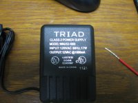
* The first photo is the transformer I used with the testing, the WAU12-1000 12Vac 1Amp transformer. If you use a 16Vac transformer it will keep the O2's voltage regulators out of dropout at maximum load current but will put 4 additional volts across the O2's voltage regulators. Which in turn means your maximum output power will be more like 1Vrms to keep the O2's voltage regulator power dissipation about the same as with the 12Vac transformer.
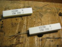
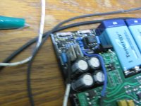
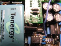
* Next two are the load resistors used, 33R at 10W, and the test setup. The green meter has a type K thermocouple attached and taped down to the top of one of the LM49600s.
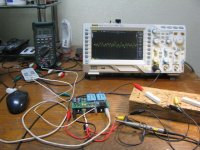
* Next is the scope shot showing 4Vpeak. Hard to see - sorry about the blur - but that is 2.00V/div in the lower left corner. The probe and multiplier menu on the screen are set up for 1X.
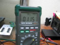
* Next photo shows the steady state temperature on top of the LME49600, 109F. No problem. Ambient is around 77F.
* Next two photos shows the thermocouple moved to the top foil, where the solder joint with the LME49600 is located: 115F. Also OK.
* Next two photos are the O2 voltage regulator at 145F. Back in 2011 I measured the heatsink of one of my O2 voltage regulators at 165 driving a 16R load and exchanged some email with NwAvGuy about it. He came back saying he considered anything under 200F OK, working back from the junction temperature. Definitely wouldn't want to touch that with your finger though!
* Next two photos shows the output level now cranked up to 7Vpeak. You can see it from that one peak on the bottom half that is just barely touching 7V. I tried running it up higher but clipping became evidient, as it should since that is all the O2 gain stage can put out. The net result is 125F on the top booster board heat sink foil, which is still OK.
I'm going to have to continue this below since I'm out of photo attachment slots...
OK, I took off early this afternoon and set up a power dissipation test rig for the O2 Booster Board with 33R loads on each channel. I believe that I've found the problem: music vs. testing with pure sine waves. NwAvGuy himself mentioned this in his blog, that if using pure sine waves the O2 headamp should only be run for 10 minutes or less at full power. The same will apply to the O2 booster board + O2 headamp combination.
In the test setup below I first used music with 4Vpeaks (2.8Vrms), then ran it all the way up to 7V peaks(5Vrms), the maximum before the O2 and the 12Vac power adaptor clip. The result: no thermal power dissipation problems at all with either the booster board or the O2's voltage regulators. I did not try the tests with pure sine waves instead of music. The power dissipation with sine waves would typically be 2x to 3x more and would likely cook both the booster board and O2's voltage regulators over time. I'll bet the dScope puts out pure sine waves. dScope or Audio Precision testing should probably be limited to 10 minutes at a whack, or preferably even just 5 minutes, before letting everything cool down.
* The first photo is the transformer I used with the testing, the WAU12-1000 12Vac 1Amp transformer. If you use a 16Vac transformer it will keep the O2's voltage regulators out of dropout at maximum load current but will put 4 additional volts across the O2's voltage regulators. Which in turn means your maximum output power will be more like 1Vrms to keep the O2's voltage regulator power dissipation about the same as with the 12Vac transformer.
* Next two are the load resistors used, 33R at 10W, and the test setup. The green meter has a type K thermocouple attached and taped down to the top of one of the LM49600s.
* Next is the scope shot showing 4Vpeak. Hard to see - sorry about the blur - but that is 2.00V/div in the lower left corner. The probe and multiplier menu on the screen are set up for 1X.
* Next photo shows the steady state temperature on top of the LME49600, 109F. No problem. Ambient is around 77F.
* Next two photos shows the thermocouple moved to the top foil, where the solder joint with the LME49600 is located: 115F. Also OK.
* Next two photos are the O2 voltage regulator at 145F. Back in 2011 I measured the heatsink of one of my O2 voltage regulators at 165 driving a 16R load and exchanged some email with NwAvGuy about it. He came back saying he considered anything under 200F OK, working back from the junction temperature. Definitely wouldn't want to touch that with your finger though!
* Next two photos shows the output level now cranked up to 7Vpeak. You can see it from that one peak on the bottom half that is just barely touching 7V. I tried running it up higher but clipping became evidient, as it should since that is all the O2 gain stage can put out. The net result is 125F on the top booster board heat sink foil, which is still OK.
I'm going to have to continue this below since I'm out of photo attachment slots...
Attachments
-
 IMG_2784.JPG180.7 KB · Views: 117
 -
 IMG_2783.JPG144.6 KB · Views: 106
 -
 IMG_2782.JPG137.7 KB · Views: 119
 -
 IMG_2770.JPG215.1 KB · Views: 328
 -
 IMG_2769.JPG174.1 KB · Views: 324
 -
 IMG_2768.JPG156.1 KB · Views: 344
 -
 IMG_2788.JPG153 KB · Views: 102
 -
 IMG_2787.JPG168.7 KB · Views: 113
 -
 IMG_2785.JPG133.4 KB · Views: 105
 -
 IMG_2790.JPG123.4 KB · Views: 103
Last edited:
Booster board power measurements, part 2
JDS Labs had noted in their testing that the output jack gets warm. That is correct! Remember that the thermal vias around the LME49600 chip transfers the heat to the booster board bottom foil. The bottom foil goes the whole length of the board including right over the output jack.
I put the thermocouple on the metal output plug to quantify the temperature rise. The photo shows about 88F vs. 78F ambient, so about 10 degrees F with a 7Vpeak output signal into the 33R loads, the maximum output signal for the O2 + booster board combo. But remember this is with real music, not sine waves. If the dScope was putting out pure sine waves I wouldn't be surprised if that output jack and plug got downright hot during the dScope testing. Thanks again to JDS for noting that!! Anyone doing pure sine wave testing on the booster will be best off letting it cool down after 5 or 10 minutes. But with actually music everything is fine long term, as all these steady-state temperature readings show.
I once again want to thank John at JDS for testing the booster board with the stock OPA140 chip. Very very helpfull! A lot of time and effort goes into setting up those tests.
Now that we know the dScope THD+N is no worse than the stock O2 with the booster board, I'm quite curious if using a dual LME49990 adaptor in for the O2's NJM2068 chip along with an OPA827 version of the booster board can significantly beat the stock O2's THD+N numbers at normal listening levels (not near maximum output). If anyone out there has an Audio Prescision or dScope tester and would like to give that one a try, just PM me and I'll send you the parts.
Attachments


Last edited:
I'm also very curious to see if replacing the njm2068 with lme49990s will have any measurable effect. For the lowest distortion I would think the opa827s could be replaced with lme49990s as well at the price of slightly more offset.
I'm also very curious to see if replacing the njm2068 with lme49990s will have any measurable effect. For the lowest distortion I would think the opa827s could be replaced with lme49990s as well at the price of slightly more offset.
I'm 100% certain you are right about that (subbing the OPA827s/OPA140s for LME49990s) because that essentially reverts to what OPC is using in his "Wire" amp (LME49990 looped around a LME49600) and he has tested that with his Audio Precision analyzer. OPC's Wire measurements beat the O2 in all areas as I recall.
Layout makes a huge difference though and it is entirely possible I've mucked something up with the layout that would result in slightly higher crosstalk, IMD, noise, etc. so I wouldn't expect exactly the Wire measurements (OPC is better at this stuff than me by a long shot!), but should be in the general vicinity - better than the stock O2 - with the trade-off of the additional higher output offset like you say.
I picked the OPA140 and OPA827 for the booster board because I had minimizing the output DC offset at the top of my design list. Those are both FET input chips (essentially no voltage drop across the O2's 40.2K resistors), along with being DC precision. The LME49990 is bipolar so much higher input bias current (resulting in higher DC output offset voltage), but lower THD+N. But the ability for someone to use the LME49990 was one of the things in the back of my mind, and is another reason why I went with two single op amps rather than one dual. You could have dual LME49990s on the adapter board in for the NJM2068, then LME49990s in for both the booster board op amps. The DC offset would probably still be lower than the stock O2 since the LME49990 has lower input offset voltage.
That music vs. sine wave issue is probably why I've never read any posts about OPC's Wire amp overheating. That kind of broke my brain when JDS Labs ran into that heating problem since I knew the booster board foil around was about the same as the Wire. Took me a while before I remembered the pure sine wave heating issue. Lol - in some PMs with NwAvGuy way back when I was always the one making a case that an amp should be able to withstand continuous sine wave testing and he was the one not buying it. Then I go and make a circuit too that won't withstand continuous sine waves. 😛
I wouldn't worry to much about the buffers overheating during sine wave testing. It won't be an issue with music for 99% of the headphones out there. I could be wrong but I think early versions of the Wire had some sort of heatsinks which aren't used on the current version and I haven't heard anything about them overheating. What I find most interesting about the booster board is that even though it isn't putting out any more power into my HD580s then a stock O2 it subjectively sounds like a more powerful amp. I guess it could be my imagination but it looks like not the only person to notice that the HD580/HD600 sounds better with the booster board. Very curious to see the distortion measurements with a better opamp in place of the njm2068.
Fsatsil - good thoughts! The booster board does provide for more dynamic headroom in terms of peak current avalability. The maximum current of the NJM4556A output chips in the O2 is around 70mA, for 140mA for the pair. The LME49600 are good for 250mA each, and although you can't run them continuously with anywhere near that much current, you can have musical peak currents much higher than the stock O2.
Pretty much from day one in the build instructions I've said that if 140mA (70mA per chip) is the maximum continuous for the stock O2, as NwAvGuy posted in his blog, then with the booster board you should be able to continuously do around 180mA, or 90mA per chip. But... for short musical peaks it can go all the way to 200mA and for very short peaks up to the 250mA. I posted a set of photos in the thread here a few months ago, using an external power supply and desktop speakers, that verified there is no problem with peaks at 250mA with the booster board.
It sounds like John at JDS Labs and I have had a miscommunication somewhere on along the way on what it is that the booster board is intended to do. It is NOT intended to run the LME49600 chips at anywhere near their full output power capability. The top goals for the booster board have been:
1. Lower distortion and noise based on the datasheet numbers for the OPA140 + LME4600 combo and, better, the OPA827 + LME4600 combo, and then both of those with the NJM2068 replaced with the LME49990 adapter board. And with those numbers at the same Vrms output levels that NwAvGuy used in his tests for the O2, which at 32 ohms is about 4.25Vrms with sine wave testing. The one dScope test John sent me was with the OPA140 + LME49600 into 150 ohms and it showed the THD+N just slightly better than the O2 amp. So the good news is I didn't make the THD+N any worse. But the bad news is that I was hoping is would be significantly better than the O2 based on the datasheets and NwAvGuy's comments in his blog that the O2's THD+N was limited by the NJM4556A chips. I was quite surprised to learn that the OPA140+LME49600 combination (with the 150R load) didn't signifantly beat the stock O2's NJM4556A chips, even with the NJM2068 left in for the gain chip!
So the big discoveries from John's testing are that the NJM4556A is apparently even better than NwAvGuy thought, which is probably good news for the ODA since that is the same chip in a different package, and that the THD+N may actually be limited by the O2's NJM2068 gain chip instead of theNJM4556A chips. So hence the importance of trying the test with the LME49990 adaptor in place of the NJM2068, in all the cases: NJM4556A chips (original O2 output), OPA140+LME49600, and OPA827 + LME49600. I'm still quite eager to see dScope or AP THD + N tests results here at normal listening levels, such at 1Vrms into 32R or 150R, to see if the THD+N really is reduced over the stock O2, and would be happy to send boards out to anyone with a recent model dScope or AP to test. Again, that test should be up to 4.25Vrms maximum into a 32 ohm load if using sine waves, and even then testing with sine waves may need to be limited to 10 minutes at a whack, as NwAvGuy wrote for the stock O2. But I'm less concerned abouut the numbers at maximum output than at normal listening levels.
I'm still hoping that the OPA827 + LME49600 combo and an LME49990 adaptor in the for the NJM2068 will come up with significantly reduced THD+N over the stock O2. 🙂 If it doesn't then my hat is definitely off to NwAvGuy and the stock O2! At that point the usefullness of the booster board would no just be the following points below.
2. No-thump relay. No turn-on or turn-off thumps. Improved THD+N completely aside, this function alone is usefull if the booster board is proven not to degrade the basic O2 THD+N, which apparently is the case at 150R.
3. Vastly lower DC output offset which may make a difference for some sensitive IEMs. Again, as long as the booster board doesn't make the stock O2's THD+N any worse, another useful function.
4. Slighly more continuous output current with a great deal more peak (burst) current for musical peaks. At 180ma total that would be 90mA per chip continuous vs. 70mA per chip half with the stock O2.
5. LEDs after the mosfets to show when the O2 mosfets are on or off and that both power rails are up
6. In the latest V3.1 schottky power rail clamp diodes, something that really should have been on the O2 given that one O2 mosfet is coming on before the other.
7. Higher slew rate. The stock O2 should be around 3V/uS. With the NJM2068 gain chip as the limiting factor, the booster board should give around 6V/uS. With the NJM2068 replaced by the LME49990 adaptor the full 20V/uS of that chip and the booster board chips should result. As NwAvGuy pointed out in his blog, 3V/uS should already be in excess of what the digital audio recording chain limits the slew rate to. But regardless I know that some folks would prefer a higher slew rate.
What the booster board is definitely not designed to do, and has never been a goal, is to run higher than the 4.25Vrms in 32 ohm with sine wave testing that NwAvGuuy shows in his blog graph as the maximum output for the O2. I haven't tried it yet, but I suspect the booster board could indeed be cranked higher to 6 or the full 7Vrms output swing into 32R with sine waves since it has larger output transistors than the NJM4556A, and does not internally current limit at around 90mA like the NJM4556A half-sections. And that would definitely cause it to overheat. But again, not a problem, since the actual usage of the booster board is music and not sine waves. As my previous posts shows music can peak up to 7Vrms with no resulting heating problems. It just means that that sine wave testing at the maximum 4.25Vrms into 32R will probably have to be limited to 5 or 10 minutes then allowing the chips to cool.
So the one thing the booster board is not intended to be is a solution for low impedance & low sensitivity headphones for the O2 headamp. I doubt there would be any way to fit a solution for those into the tiny B2-080 case for that matter. For that it would take the ODA, AMB's b22, or any other headamp designed for that much voltage swing and current.
Last edited:
My booster board has developed a small turn on/off sound like a click through the right channel when the relay turns on and off. Any idea what would cause this? It has never done this before it was always completely silent when I turned it on or off.
My booster board has developed a small turn on/off sound like a click through the right channel when the relay turns on and off. Any idea what would cause this? It has never done this before it was always completely silent when I turned it on or off.
Measure your DC output voltage again on both channels with the input cable disconnected (inputs grounded). DC on the output can cause that. Are you using the OAP140 chips? Remember that you have to wait that 5 seconds for the relay before the output voltage shows up - lol, I forget about that myself when testing. 🙂
Also are both of your green LEDs on and about the same brightness? Unbalanced power rail voltages can do that too, although it would usually affect both channels.
I've probably forgotten to post along the way that part of the super-silent turn on and turn off is having that DC output offset voltage so low, along with the relay.
Last edited:
This is so strange it happened all of a sudden. I checked the DC offset a week or two ago and it was so low my meter couldn't read it and now I have a dc offset of around 50mv on one channel! My batteries are both reading 9.37v so it's not unbalanced rails and both LEDs are on and the same brightness. I haven't changed a thing since i tested the dc offset a week or two ago and the amp has been working perfectly up until yesterday when it started making the turn on/off noise.
Ok I swapped out the opa140s for a different pair of opamps and I still have the offset on one channel so I thinking it is most likely one of the buffers. I have one spare lme49600 I can try but first I need to figure out which one on the board is the bad one. Which is the right and which is the left buffer?
Ok I swapped out the opa140s for a different pair of opamps and I still have the offset on one channel so I thinking it is most likely one of the buffers. I have one spare lme49600 I can try but first I need to figure out which one on the board is the bad one. Which is the right and which is the left buffer?
IC2, the one closest to the batteries, and IC1 are the right channel.
I would recommend going through the procedure in post #150 at this point for IC2 and IC1, which breaks the loop between the buffer and op amp to test each individually. 50mV is still within the normal input offset voltage for the buffer (it can go up to 60mV) with its input grounded. I'm guessing that IC1 is still not doing its thing for some reason. The procedure in post #150 will measure that too, the output of IC1 with the loop broken. But first, measure one more thing. Measure what you get on either side of R1 to ground. It should be zero, unless IC1 is shorted inside, or 50mV is coming up from the O2 PC board.
Last edited:
Ok I measured from R1 to ground and I'm getting about 3mv on the side if the resistor closest to the buffers and 0 on the other side. I also tried switching the opamps from left to right and nothing changed so It looks like the opamp is not bad. Would you reccomend I swap out the buffer next or should I still go through the procedure in post #150? Thanks for all your help!
Ok I measured from R1 to ground and I'm getting about 3mv on the side if the resistor closest to the buffers and 0 on the other side. I also tried switching the opamps from left to right and nothing changed so It looks like the opamp is not bad. Would you reccomend I swap out the buffer next or should I still go through the procedure in post #150? Thanks for all your help!
I would still go through the test procedure. It will provide some useful info and involves cutting pin 2. To get the buffer out you would probably want to snip all 5 pins anyway, desolder the tab, then go back with solder wick and clean the leg remnants from each of the 5 pins.
The first part of that procedure is cutting/lifting (but don't lift too much - one fellow already found out the pin will snap off!) pin 2, grounding it, then powering up again and seeing what the output voltage is. Then next is just measuring the output voltage of the op amp with that buffer pin 2 lifted. The output of the op amp should be zero. If not, there is a bad solder connection somewhere in the parts around IC1. Keep in mind too there are some parts on the back of the board, two resistors, that feed power to IC1.
Well I followed the procedure in post #150 and I've traced the problem to the O2 board. Here's the measurements I got
Pin 2 of IC1 grounded
12mv on pin4 ic2
Ic1 pin6 output -6.15v
Ic1 pin3 input -65mv
So I pulled the buffer board and installed the njm4556 opamps back in u3/u4 and I am measuring about 65mv dc from pin3 of U3 to ground. I don't get any dc on pin 3 of U4 so it's only the right channel that's effected. I've checked the solder joints and they all look good so the only thing I can think of is that the socket is bad. Any other ideas?
Well it looks like I'm gonna have to build a new O2 I buggered up the board trying to remove the u3 socket.
So I pulled the buffer board and installed the njm4556 opamps back in u3/u4 and I am measuring about 65mv dc from pin3 of U3 to ground. I don't get any dc on pin 3 of U4 so it's only the right channel that's effected. I've checked the solder joints and they all look good so the only thing I can think of is that the socket is bad. Any other ideas?
I had something similar happen once and the cause turned out to be extremely odd. I was reading about 100mV on one channel after just installing a booster board on an O2 board that had been sitting on a shelf for awhile. I traced it down to the 100mV coming up from the O2 board also. At first that just makes no sense given the only place that input line goes on the O2 board is a 40.2K resistor to ground and the 2.2uF coupling capacitor. How could voltage get on that line?
After inspecting the board with a magnifying glass I saw a tiny bit of blueish corrosion around two of the part leads and a thin film of something transparent in one small spot on the board. Turns out I had the O2 board sitting right next to an open can of "damp rid" moisture absorber. Over the months some of that stuff had landed on the board and it turns out the stuff is conductive. It formed a high resistance path from one of the power supply lines to the the input line of the output op amp. I cleaned the board off with isopropyl alcohol and all was fixed. 🙂 You might give that a try. The booster board chips are FET input so the gate impedance is fairly high, that 40.2K resistor on the booster board.
Well it looks like I'm gonna have to build a new O2 I buggered up the board trying to remove the u3 socket.
I'm sorry to hear about that! You might be able to salvage it. The booster board only needs two of the signals out of all the 8 U3 pins IF you connect JP5 to the pin near it hanging off the end of the booster PCB, as in the photo below. That lets the booster get V+ and V- from U4.
Then you just need to wire what was U3 pin 3 on the booster board to the end of R12 on the O2 closest to the O2 red led. Then wire what was U3 pin 1 to to the end of the O2's R11 that is closest to U3.
Attachments
- Home
- Amplifiers
- Headphone Systems
- O2 headamp output booster PCB