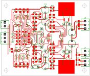
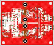
Too bad there isn't a PCB available for this design.
There was a group buy some time ago, could be done again if more interested.
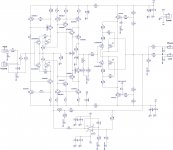
About 29 mA, defined with R30 and R31 values.
Is that continuous or peak? I'm trying to determine the SOA of some surface mount devices for there.
Is that continuous or peak? I'm trying to determine the SOA of some surface mount devices for there.
Q19 and Q20 (your schematic) dissipation does not go over 400 mW average dissipation is 320 mW.
Q17 and Q18 are the ones I'm concerned with. They are dual devices in a SOT-363 package. They look good for thermal bonding but I'm not sure how good their SOA is if they are carrying a bias current.
http://www.onsemi.com/pub_link/Collateral/BC846BPDW1T1-D.PDF
http://www.onsemi.com/pub_link/Collateral/BC846BPDW1T1-D.PDF
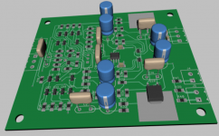
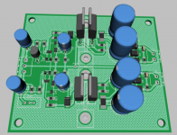
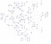
Here's what I've come up with so far.
I've found one error on your schematic, Q6, Q13 collectors(your schematic) should be connected to the ground, and there is no trimer pot.
If you want separate boards for preamp and shunt regulator in this case connection between them should have five pins terminal. Outputs from the regulator are +-15V, +-sensor, and the ground. The +-15V and +-sensor should be connected on the preamp board not on the power board.
You need +-80 mA from the power board, so calculate the SOA accordingly.
Damir
Thanks for checking my schematic. I thought R18 in your schematic was a pot. I've also got R8 connected to the wrong ground.I've found one error on your schematic, Q6, Q13 collectors(your schematic) should be connected to the ground, and there is no trimer pot.
If you want separate boards for preamp and shunt regulator in this case connection between them should have five pins terminal. Outputs from the regulator are +-15V, +-sensor, and the ground. The +-15V and +-sensor should be connected on the preamp board not on the power board.
You need +-80 mA from the power board, so calculate the SOA accordingly.
Damir
I will likely attach the shunt regulator to the preamp board. I just like to design in modules and join them later. Where would the best place be to take the +- sense from?
Last edited:
Thanks for checking my schematic. I thought R18 in your schematic was a pot. I've also got R8 connected to the wrong ground.
I will likely attach the shunt regulator to the preamp board. I just like to design in modules and join them later. Where would the best place be to take the +- sense from?
Make that connection on the preamp board or close where +-15V is entering the preamp board.
If you look mine layout than you can see that I have connected that on the shunt regulator side (but it is close to the preamp part). First I made the layout with provision of separated shunt regulator, but later decided to make all on the one board. Separated shunt regulator could be quite distanced from the preamp board and in this case is important to connect power and sense together on the preamp board.
Thanks.
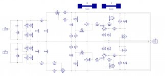
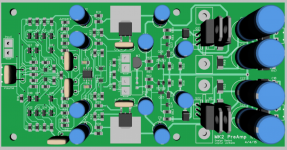
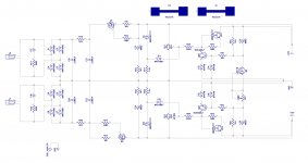
Here's the supply.
Beautifull
What software are you using to produce these results ?
Beautifull
What software are you using to produce these results ?
Diptrace.
Why did you choose that software instead of KiCAD or EAGLE ?
I am trying to choose one but know little about them so your input will be primordial.
I am trying to choose one but know little about them so your input will be primordial.
It's free up to 500 pins. I tried Eagle many years ago and didn't like it. I haven't tried it since. I've never tried Kicad.
Thank you... I will give it a try.
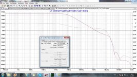
Just calculated output impedance of the mirror (just before R17) and found 1926ohms.... is it possible ?
Just calculated output impedance of the mirror (just before R17) and found 1926ohms.... is it possible ?
HN3A51F ( dual PNP) toshiba
HN3A51F(TE85L,F) Toshiba Semiconductor and Storage | HN3A51F(TE85LF)CT-ND | DigiKey
and
HN3C51F ( dual NPN) toshiba
HN3C51F-BL(TE85L,F Toshiba Semiconductor and Storage | HN3C51F-BL(TE85LFTR-ND | DigiKey
very good for this project
wht was the reason for R50 = 100k ??
HN3A51F(TE85L,F) Toshiba Semiconductor and Storage | HN3A51F(TE85LF)CT-ND | DigiKey
and
HN3C51F ( dual NPN) toshiba
HN3C51F-BL(TE85L,F Toshiba Semiconductor and Storage | HN3C51F-BL(TE85LFTR-ND | DigiKey
very good for this project
wht was the reason for R50 = 100k ??
Those appear to be dual 2SA992 and 2SC2240. Good parts, high voltage and decent rbb' (I see where I deduced that rbb' is about 30 ohms for the PNP).HN3A51F ( dual PNP) toshiba
HN3A51F(TE85L,F) Toshiba Semiconductor and Storage | HN3A51F(TE85LF)CT-ND | DigiKey
and
HN3C51F ( dual NPN) toshiba
HN3C51F-BL(TE85L,F Toshiba Semiconductor and Storage | HN3C51F-BL(TE85LFTR-ND | DigiKey
HN3A51F ( dual PNP) toshiba
HN3A51F(TE85L,F) Toshiba Semiconductor and Storage | HN3A51F(TE85LF)CT-ND | DigiKey
and
HN3C51F ( dual NPN) toshiba
HN3C51F-BL(TE85L,F Toshiba Semiconductor and Storage | HN3C51F-BL(TE85LFTR-ND | DigiKey
very good for this project
wht was the reason for R50 = 100k ??
I suppose that R50 is from my schematic, current conveyor shunt load.
I think that I explained that somewhere in this thread. Attached are two Loop Gains, with R50 and without, and I think that those pictures talk by itself.
Attachments

Last edited:

I tried Eagle many years ago and didn't like it. I haven't tried it since.
Eagle hasn't changed much. I've never liked it either.
- Status
- Not open for further replies.
- Home
- Amplifiers
- Solid State
- No NFB line amp (GainWire mk2)