A toggle switch and a pair of flanking LEDs will be fitted to the front.
Very Nice !!!


how nice they're looking ...... even if other-transparent-lacquer would allow that beauty traces could be seen
that must be drawn by some extra skillful Guy


that must be drawn by some extra skillful Guy
Zen Mod said:other-transparent-lacquer would allow that beauty traces could be seen
Thanks ZM and I 100% agree, that’s the only thing I don’t like about the Black PCBs but still they help the components be the stars of the show
Last edited by a moderator:
Cool work. Are you going for 2x6 way for each channel? Monoblocks?
Thanks, yes with an over complicated 2.5kVA transformer and 70VDC Rails, if I’m brave enough to power it for the first time!!
Hi Sir Nelson, I admire your work and designs 🙂
by the way Sir Nelson, I came across the threshold stasis 1, it badly tampered. 🙁 i am hoping if you can share with me a schematic diagram of the logic circuit and power supply vu driver for troubleshooting reference. 🙂
by the way Sir Nelson, I came across the threshold stasis 1, it badly tampered. 🙁 i am hoping if you can share with me a schematic diagram of the logic circuit and power supply vu driver for troubleshooting reference. 🙂
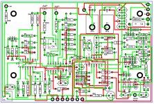
I matched all FE transistors, even the ones that didn’t need to be matched... I used 10mA Idss JFETs and they were the only 4 I had on that range, I’m wondering if I should use lower Idss ones which I have a bunch and leave these for a future more demanding design, what you guys think?
Oh... the little SMD JFETs on the bottom are to be used in case the 2SK170s can’t be found right?


Oh... the little SMD JFETs on the bottom are to be used in case the 2SK170s can’t be found right?
... I’m wondering if I should use lower Idss ones ...
Yes you can: they're designed to run at 2mA each.
agree with Zung - I wrote that few times in thread, when boyz asked
and yes - either 2Sk170 (GR, BL, V, whatever) or 2SK2145
though, one can try putting them all
I didn't yet tried that
and yes - either 2Sk170 (GR, BL, V, whatever) or 2SK2145
though, one can try putting them all
I didn't yet tried that
i am hoping if you can share with me a schematic diagram of the logic circuit and power supply vu driver for troubleshooting reference. 🙂
Here is what I have.
Attachments
...
though, one can try putting them all
I didn't yet tried that
That'll be a REAL PROJECT for REAL MAN: 1000 Fet FE, 1000 Fet OS.
What are you wanting for?
🙂
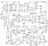
Oooh the RC4136 quad (!!) opamp by Raytheon. Used extensively in the Phase Linear 2000 preamp, which made its debut in 1975.
Oooh the RC4136 quad (!!) opamp by Raytheon. Used extensively in the Phase Linear 2000 preamp, which made its debut in 1975.
You laugh, I had some of those from ESS, and made a nice little preamp.
😱

- Home
- Amplifiers
- Pass Labs
- New Stasis front end