I'm thinking of a L shape AL clamp: fewer holes to drill (my worst nightmare), better distribution of the pressure.
when mildly dissipating devices are in case ( as in Stasis) , "good enough" is not critical
in FW style amps, in cases of having close to 40-50W of heat per device, every eenytiny detail , leading to better thermal interface, is important
in FW style amps, in cases of having close to 40-50W of heat per device, every eenytiny detail , leading to better thermal interface, is important
when mildly dissipating devices are in case ( as in Stasis) , "good enough" is not critical
in FW style amps, in cases of having close to 40-50W of heat per device, every eenytiny detail , leading to better thermal interface, is important
Agreed!!!


looking nice .... and tight
just don't ook drive polarity to secondary OS pcb
remember - make X shape

just don't ook drive polarity to secondary OS pcb
remember - make X shape
looking nice .... and tight
just don't ook drive polarity to secondary OS pcb
remember - make X shape
Yes Sir!!!
Some progress. One channel comes up and I can adjust the bias. Sadly the other channel sits at 0mV across the emitter resistors and no amount if pot fiddling gets it to move. Rail voltages are -/+32Vdc and there's no short to ground.
No magic smoke though. 🙂
No magic smoke though. 🙂
Last edited:
well, that one channel confirms that nothing on my side is ooked up
I believe root of your problems is - you didn't post enough porn, prior to powering up
I believe root of your problems is - you didn't post enough porn, prior to powering up
well, that one channel confirms that nothing on my side is ooked up
I believe root of your problems is - you didn't post enough porn, prior to powering up

Porn only if you've been good...🙂
Took the FE board off and powered it separately. D+ and D- stuck at the negative rail. Tweaking the offset pot I managed to get -/+D to about -/+9Vdc, still not right. Tweaking the bias pot made very little difference to the voltages on -/+D.
I've started to desolder transistors. The two drivers in the heatsinks are fine, as is the 550 between them.
I've also checked components and values against the working FE board, and the boards as the same. Can't see any solder bridges either.
I'll keep unplugging transistors.
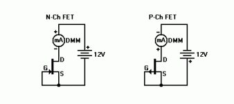
Could it be the JFETs I wonder?
Took the FE board off and powered it separately. D+ and D- stuck at the negative rail. Tweaking the offset pot I managed to get -/+D to about -/+9Vdc, still not right. Tweaking the bias pot made very little difference to the voltages on -/+D.
I've started to desolder transistors. The two drivers in the heatsinks are fine, as is the 550 between them.
I've also checked components and values against the working FE board, and the boards as the same. Can't see any solder bridges either.
I'll keep unplugging transistors.
Could it be the JFETs I wonder?
Some pictures...
For testing the transistors I'm using this little beastie

Front side

Solder side

OS Board

OS and FE board

Not made much progress today. Still desoldering transistors and checking.
Any help would be very much apprecaited.
For testing the transistors I'm using this little beastie
Front side
Solder side
OS Board
OS and FE board
Not made much progress today. Still desoldering transistors and checking.
Any help would be very much apprecaited.
can't help much, except listing regular things
- orientation of semis
-placement of semis
-all proper resistor values in place
-switch checked ( put short for testing)
-thermistor in place, checked cold?
-trimpots checked
- orientation of semis
-placement of semis
-all proper resistor values in place
-switch checked ( put short for testing)
-thermistor in place, checked cold?
-trimpots checked
Thank you ZM for the pointers.
But I did find the mistake.
The very last transistor I took out, J2...up until then every single one of those little slices of doped silicon tested good...
And then there was J2...it wasn't an 2SK170 shall we say!
Time to clean the board and re-solder 🙂
I can't wait to hear this amp.
But I did find the mistake.
The very last transistor I took out, J2...up until then every single one of those little slices of doped silicon tested good...
And then there was J2...it wasn't an 2SK170 shall we say!
Time to clean the board and re-solder 🙂
I can't wait to hear this amp.
Without doubt I have the relished prize of Omnidumb.nice try..... but we all know who's here Omnidumb, owner of silliest mistakes
However I also have a second channel adjusting nicely and warming up the heatsinks. *Basking in the radiant heat of 600mA of bias*
Just noticed that the drivers on the FE board get too hot to touch, even for a second, and that's with the lid off. Gonna have to find bigger heatsinks.
check voltage across 33R in positive rail - expect something as 0V55-0V6
meaning Iq~17mA
meaning dissipation per critter around 0W55, with your 36-ish rails
if yup for all, heatsinks are OK, your digits are tender 🙂
meaning Iq~17mA
meaning dissipation per critter around 0W55, with your 36-ish rails
if yup for all, heatsinks are OK, your digits are tender 🙂
Just noticed that the drivers on the FE board get too hot to touch, even for a second, and that's with the lid off. Gonna have to find bigger heatsinks.
Interesting, I wonder how are mine going to behave with 70V rails...
dunno did I mentioned that, but I believe your build deserves and need dedicated thread
can't track what we spoke about changes and choices
I remember writing something, but tricky to check back
can't track what we spoke about changes and choices
I remember writing something, but tricky to check back
- Home
- Amplifiers
- Pass Labs
- New Stasis front end