Not really, but it might not be very important.
Ok John,
but after some simulations, I realized that keeping the connection of the emitters of the PNPs only, ( removed of the NPNs ), that change beyond increase Open Loop Bandwidth, the noise level remains the same as the original.
I know that is just a simulation but up to now it don´t " lied " to me, in this case.
eD
Missing connection
I don´t think so !
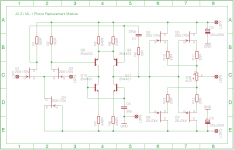
There is no biasing for the NPN transistors as shown on the post #212 ( and #213 ). Wrong connection!
Schematic looks generally OK.
I don´t think so !
There is no biasing for the NPN transistors as shown on the post #212 ( and #213 ). Wrong connection!
I think the connection between R8 and R9 should be removed (John said so, although he said it would work either way.) I suppose you used Toshiba FETs instead of the Fairchild in the schematics. What is the current through the input FETs (voltage across R1 or R2) ? I think the current source would need some adjustment. Did you try to lower the values for R11 to R14 ? I would lower R11 to R14 to 20R each and VR1 to 50R as a start. But I did not try that yet - just an idea.
Hi gk7
I measured the voltage across R1 & R2 = 8.6v
I use 2N5459 & 2N5462 because I have problem to get 2SK170v & 2SJ74v here in my place.
I will try to lower the value for R11 and R14 also VR1. I will advice result.
Would like to know what is the best idss for the JFets at input and ouput stages.
Attachments
Hi I am getting J74V/K170V for this build, can you send me the actual circuit and values - also any idea of the pcb ? would be great.
thanks- youcan PM me or email kannan_srinvasa at yahoo dot com
kannan
Hi kannan
I can send you a set of phono pcbs for stereo if you want. Let me know.
Hi gk7
I measured the voltage across R1 & R2 = 8.6v
I use 2N5459 & 2N5462 because I have problem to get 2SK170v & 2SJ74v here in my place.
I will try to lower the value for R11 and R14 also VR1. I will advice result.
Would like to know what is the best idss for the JFets at input and ouput stages.
Hi HCK,
you said you used the original values so R1 = R2 = 100 Ohms. 8.6V through them would be 86mA which is way too much. Are you sure or is this a typo ?
My datasheets for the 2N5459 & 2N5462 say they are Idss 4-16mA, BTW.
8.6V sounds about ten times to high to me.
Hi gk7 & John
I measured the voltage across each resistor again @ +/- 13v rail:
R1 = 8.1v
R2 = 8.1v
R3 = 3.98v
R4 = 4.69v
R5 = 0v
R6 = 7.39v
R7 = 7.37v
R8 = 7.33v
R9 = 7.34v
R10 = 0v
R11 = 0.2v
R12 = 0.2v
R13 = 0.2v
R14 = 0.2v
Schematic is here:
Please comment, thanks
I measured the voltage across each resistor again @ +/- 13v rail:
R1 = 8.1v
R2 = 8.1v
R3 = 3.98v
R4 = 4.69v
R5 = 0v
R6 = 7.39v
R7 = 7.37v
R8 = 7.33v
R9 = 7.34v
R10 = 0v
R11 = 0.2v
R12 = 0.2v
R13 = 0.2v
R14 = 0.2v
Schematic is here:
Please comment, thanks
Attachments
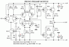
16mA passing R3.
This should result in 818mV (~8mA) across the drain resistors.
Vr4 + Vr5 =26V. You measure 0V+4.69V
Some thing is seriously wrong with your measurements or your circuit.
This should result in 818mV (~8mA) across the drain resistors.
Vr4 + Vr5 =26V. You measure 0V+4.69V
Some thing is seriously wrong with your measurements or your circuit.
Last edited:
Hi HCK,
to summarize our "findings" so far:
As John, Andrew and me already pointed out the drain currents
are off by approximately ten times, somethings broken here.
I would check:
- The current source: Measure if you get the 16mA through
R3 that Andrew indicated, if not you will have to check the
resistors for correct values and replace the FET
- The two FETs of the input stage: They are probably already broken
too, they should be checked and replaced if needed.
For the FETs:
As mentioned before the FETs you use (2N5459 & 2N5462) are specified with Idss 4-16mA,
you will at least have to select them for high Idss and probably consider
other (higher Idss) FETs for the current source.
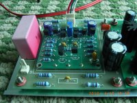
Hi Gents
I changed R1 & R2 to 1K instead of 100 Ohm. Others remain unchanged. Now the offset is much lower than before. It is drifting between 50 ~ 100mv.
Please comment.
I changed R1 & R2 to 1K instead of 100 Ohm. Others remain unchanged. Now the offset is much lower than before. It is drifting between 50 ~ 100mv.
Please comment.
HKC, 8V across a 100 ohm resistor implies 80 ma from the E110, yet I designed the circuit to be about 15 ma from each E110. Sometimes computer simulations make crazy results. I found out about this in 1966, and almost got fired for it.
Hi John
Thank you for the information, I know 80ma is definately too much for the input stage.
I would be pleased to know if the schematic I posted has any drawing error. I believe with a correct schematic the problem can be fixed.
Thank you for the information, I know 80ma is definately too much for the input stage.
I would be pleased to know if the schematic I posted has any drawing error. I believe with a correct schematic the problem can be fixed.
You must use 100 ohm or less for the input load resistors. The circuit will not work properly with more.
Hi John
What is the bias current for 2nd & output stage on the original design? I measured voltage across resistors R6/R7/R8/R9 7.4v/243 Ohm = 30.45ma and resistors R11/R12/R13/R14 0.2v/60.4 Ohm = 3.3ma.
What is the bias current for 2nd & output stage on the original design? I measured voltage across resistors R6/R7/R8/R9 7.4v/243 Ohm = 30.45ma and resistors R11/R12/R13/R14 0.2v/60.4 Ohm = 3.3ma.
HKC, I think you are outside your scope of competence with this circuit. Please do NOT modify it. The problem is that you changed the 100 ohm resistors to 1K without understanding what you did. Now, please return them to 100 ohms, and all will be well.
Last edited:
Hi John
Thank you for your quick response.
I am not intended to modify the circuit. Actually I prefer to clone it original. I will change the drain resistors back to 100 Ohm and parrelle the JFets to get enough idss which you said is 15ma.
Thank you for your quick response.
I am not intended to modify the circuit. Actually I prefer to clone it original. I will change the drain resistors back to 100 Ohm and parrelle the JFets to get enough idss which you said is 15ma.
Just change the output resistors to 20 ohms or so. You have too much resistance for the Gm of the output devices that you are using. Please understand, the E110 is a big fet, AND it is NOT made today. The E212 and the E175 are not made in the same package AND the better part, instead of the E212 is the J113 with 20 or more ma, Idss. You are using parts that do not resemble the original parts. SOME changes should be made, but NOT the change that you made. Please remember, this design is 37 years old.
Last edited:
- Home
- Source & Line
- Analog Line Level
- Need to build JC 2 preamp