Looks ok as far as I can tell, you can ignore the JP1 waning. I usually tick the 'track errors' & 'schematic parity' boxes in the DRC as well, just to make sure I'm picking everything up.
Ah - just noticed R423 again - it's showing the grey/white "R423" on the fabrication layer, but there's no yellow R423 part reference on the F. Silkscreen layer (it's the yellow labels that appear on the final pcb). That's the problem I noted before, so just follow the instruction in the bottom para of post #217 to turn the part ref. on and position it.
Ah - just noticed R423 again - it's showing the grey/white "R423" on the fabrication layer, but there's no yellow R423 part reference on the F. Silkscreen layer (it's the yellow labels that appear on the final pcb). That's the problem I noted before, so just follow the instruction in the bottom para of post #217 to turn the part ref. on and position it.
hi, ok thats all doneThese are the requirements you'll need to use for JLCPCB (other pcb producers are likely to be subtly different) - just copy the screens shown in the pdf file. They may not all be perfect, but they work (for this).
Once those are changed in your Kicad, you'll need to make sure your 'Text' items (e.g., any text on the silkscreen layers, part #'s, etc.) are the correct dimensions - most of your text thicknesses will be wrong. Just use the Edit - 'Text & Graphics Properties' page to correct the thickness value (as per the attached screen) - on any layer with text items showing.
View attachment 1412798
Then check the DRC tool - it probably won't like your C403 reference, just correct that. You also seem to have some 'spurious' (?) R423 text item showing in white/grey on the edge of the pcb - just double click the R423 part symbol (to open it's properties page), tick the 'show' box next to the R423 reference, and OK. That should revert it to yellow text (on the F. Silscreen layer) so you can move it back onto the pcb.
After that, you should only have 1 error showing in the DRC check - for the jumper.... then the fun can start with the connection tabs.
See if you can find how to set the Ground plane 'priority', it may be needed (if you find it, set it to 0).
having a bit of trouble with this bit.I presume you use the filled area tool but how do you get the exact size?

Just start by drawing say a 2.25mm wide section of track somewhere off to the side of the pcb - if you don't have a 2.25mm track width, just right click and add one to the tool first. Use the B.Cu layer, the track tool, and a 0.25mm grid:
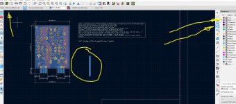
Switch to the 'Filled Area' tool, and just draw a rectangular filled zone over the section of track (zoom right in to pixel level to make sure it's rectangular) - the dimensions are irrelevant. Set the zone net to 'no net', and priority to 0 as you start drawing it:
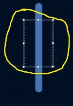
Now click on one edge of the zone to highlight the zone outline, then just use the mouse to drag and drop one edge of the zone exactly onto the edge of the underlying 2.25mm wide track (click and hold the middle point of the edge to grab & drag it). Zoom right in to pixel level to get it exactly on top of the track edge. Repeat for the other side of the zone, and you should end up with a zone exactly 2.25mm wide, on top of the track segment. Delete the track segment, it's no longer needed. Don' worry about the length of the zoen.
 like this:
  then this:
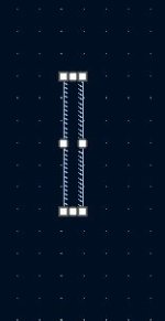
Now switch to the B.Mask layer, and repeat the process, to add a filled (B. Mask) zone exactly on top of the B.Cu. zone you've just made. Again, don't worry about the length of the zone - except - once you've set the width, you should drag and drop the top of the zone so both tops align. Note - the different colours of the 2 zones, denoting the different layers they are on, and that you don't set nets or priorities for the mask zone.
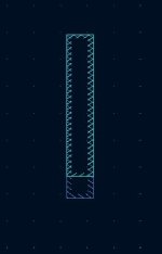
The rest of the instructions I already posted should then apply.

Switch to the 'Filled Area' tool, and just draw a rectangular filled zone over the section of track (zoom right in to pixel level to make sure it's rectangular) - the dimensions are irrelevant. Set the zone net to 'no net', and priority to 0 as you start drawing it:

Now click on one edge of the zone to highlight the zone outline, then just use the mouse to drag and drop one edge of the zone exactly onto the edge of the underlying 2.25mm wide track (click and hold the middle point of the edge to grab & drag it). Zoom right in to pixel level to get it exactly on top of the track edge. Repeat for the other side of the zone, and you should end up with a zone exactly 2.25mm wide, on top of the track segment. Delete the track segment, it's no longer needed. Don' worry about the length of the zoen.
 then this:
Now switch to the B.Mask layer, and repeat the process, to add a filled (B. Mask) zone exactly on top of the B.Cu. zone you've just made. Again, don't worry about the length of the zone - except - once you've set the width, you should drag and drop the top of the zone so both tops align. Note - the different colours of the 2 zones, denoting the different layers they are on, and that you don't set nets or priorities for the mask zone.

The rest of the instructions I already posted should then apply.
so i get to this part ok

but when i get to the part of dragging one edge i get this

if i try and do the same with the other edge it moves the whole thing over the other side it just does this.I have follwed your instructions

but when i get to the part of dragging one edge i get this
if i try and do the same with the other edge it moves the whole thing over the other side it just does this.I have follwed your instructions
3 corners of your filled zone are wrong - correct them, and it should work fine.zoom right in to pixel level to make sure it's rectangular
It's quicker and easier to add the B.Mask zone before grouping and copying - now you have to add 6 B.Mask zones....
just out of interest how did you mark up with the dimensions?Let me take a look at the zip file - you shouldn't need to change more than a couple (at most) of the footprints on the pcb screen, the pad & hole sizes of the std f'prints are correct. That is quite likely to cause problems. I think the only f'print I had to change was the jumper.
Note: there's one important aspect we've not covered at all yet, the JLCPCB production 'requirements', e.g., their mechanical production constraints. The pcb has to satisfy those as well, and they dictate track dimensions, clearances between pads tracks, vias, text sizes & thicknesses, etc. etc - those values are what the 'DRC' tool is actually comparing your pcb data to (DRC = Design Rule Constraints). All of the parameters required for the production line equipment are changed on only 1 or 2 screens, so it's far less daunting than it sounds & I can give you a set of values to use & you can see the current Kicad values on the following pages:
FILE - BOARD SET-UP - DESIGN RULES (the JLCPCB values differ only slightly from the Kicad defaults, but will need to be change at some point)
Your snapshot above seems to be showing the 'Edge Cuts' layer (where the cuts will appear in white/grey according to the colour in the small box where it says 'Edge Cuts') - but there's no white/grey edge cuts on the pcb itself. I suspect you may have drawn them on the F.Cu layer instead (the outer 'box' in your image is red).
If it helps at all - this image is essentially correct, albeit with a couple of modifications - the white 'box' around the outside is the edge cuts layer (ignore the marked dimensions, those are only temporary).
View attachment 1412357
For the dimensions - on the top menu's, select 'Place', then 'Add Dimension'. You also have dimensions & ruler tools on the bottom of the menus by the appearance manager (right of the screen).
How's the pcb going now, it should be almost finished ?
How's the pcb going now, it should be almost finished ?
- Home
- Amplifiers
- Solid State
- NAD 3030 complete rebuild
