OK - try this for the schematic corrections:
(1) Note especially the 'Vee' connections - that's a significant change.
(2) I'm not sure why, but the 'ERC' is not liking the triangular ground symbol (hence the warning you've been seeing by C423) - so just change all the 'GND' labels (5x) as shown.
It should then be ok - you could add the 2 'missing' caps described in post #82 (that are on the back & bottom of the pcb, but it's up to you - they could also be added later).
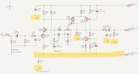
(3) I had a quick look at your assigned 'footprints' - you should probably check the exact part 'dimensions' you want to use, several of the caps esp. seem a little 'small' (Mouser is useful for exact part sizes). If the final pcb doesn't have enough 'space' allocated for any part, it'll be a problem... The resistors are probably fine, but you could also use 'vertical' resistor footprints if you're trying to gain some real estate, it saves a bit, but again, up to you.
(4) On your pcb - you actually have 2 planes drawn - a red one on the Front Copper (F.Cu) layer, which is presently assigned as the ground layer (but which is not needed at all), and a blue one on the bottom copper (BCu) layer that has no net assignment. Just select the red plane and delete it, then select the blue plane, right click, and assign it to the GND net via it's 'properties'. That should sort the planes out for now (just make sure the pcb outline is larger than the plane outline. I had the same problem when I started... trying to remember which layer I was working on. The colours shown in the 'appearance manager' on the RHS of the screen help.
(5) Once that's done - just select 'tools', 'Clean up tracks & vias', then 'build changes', and then 'update pcb' - that'll clean the tracks up a bit.
(6) Now, select the 'Update PCB from Schematic' button, 'Update PCB', and then press button 'B' to refill the plane - you should then see the missing net connections which still need to be routed.
I'll leave you to fill in the other tracks (again - ignore any pads marked 'GND' or 'Audio Ground', and delete anything marked 'Supply Ground' if there is) - it'll help if some parts are moved slightly / turned.
(1) Note especially the 'Vee' connections - that's a significant change.
(2) I'm not sure why, but the 'ERC' is not liking the triangular ground symbol (hence the warning you've been seeing by C423) - so just change all the 'GND' labels (5x) as shown.
It should then be ok - you could add the 2 'missing' caps described in post #82 (that are on the back & bottom of the pcb, but it's up to you - they could also be added later).

(3) I had a quick look at your assigned 'footprints' - you should probably check the exact part 'dimensions' you want to use, several of the caps esp. seem a little 'small' (Mouser is useful for exact part sizes). If the final pcb doesn't have enough 'space' allocated for any part, it'll be a problem... The resistors are probably fine, but you could also use 'vertical' resistor footprints if you're trying to gain some real estate, it saves a bit, but again, up to you.
(4) On your pcb - you actually have 2 planes drawn - a red one on the Front Copper (F.Cu) layer, which is presently assigned as the ground layer (but which is not needed at all), and a blue one on the bottom copper (BCu) layer that has no net assignment. Just select the red plane and delete it, then select the blue plane, right click, and assign it to the GND net via it's 'properties'. That should sort the planes out for now (just make sure the pcb outline is larger than the plane outline. I had the same problem when I started... trying to remember which layer I was working on. The colours shown in the 'appearance manager' on the RHS of the screen help.
(5) Once that's done - just select 'tools', 'Clean up tracks & vias', then 'build changes', and then 'update pcb' - that'll clean the tracks up a bit.
(6) Now, select the 'Update PCB from Schematic' button, 'Update PCB', and then press button 'B' to refill the plane - you should then see the missing net connections which still need to be routed.
I'll leave you to fill in the other tracks (again - ignore any pads marked 'GND' or 'Audio Ground', and delete anything marked 'Supply Ground' if there is) - it'll help if some parts are moved slightly / turned.
I already posted a 'map' in post # 163, that was produced from the schematic you should have now...
As I've said a few times now, you need to look at alternative possible 'routes' to solve track crossing problems - rotating parts so you can route 'through' them will help, e.g, your R429, C405, etc. - use the map in post #163 as a guide.
You also seem to still be routing various GND pads - don't forget to press the 'B' key on your keyboard every time you do anything that affects the ground plane - that refills the plane & reconnects all the ground terminals to the ground plane. If you don't do that, you'll end up chasing remnants of the ratsnest for weeks... e.g., the track you've draw between R519 and C424 (delete that track completely, and then press 'B' and you'll see what happens) - I am assuming the plane on the bottom of the pcb has been assigned to the 'GND' net.
There should be only ONE track crossing issue that can't be readily resolved, that does require the use of the wire-link 'jumper' (as discussed in post #154, point (2)) - follow the instructions there to add the jumper to the schematic, and get it onto the pcb screen.
Once it's on the pcb screen you can 'edit the footprint' directly (just off to the side somewhere, so it's not interfering with the rest of the pcb while you work on it) - to give it a suitable size (pad separation), as follows:
- Select it, right click, and open it in the footprint editor
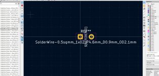
- drag and drop the 3 bits you don't need out of the way (for now)
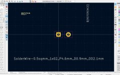
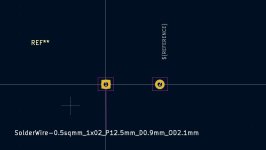
- now just drag & drop the other 3 bits back to about the same positions as before (ideally you should also edit the long text entry, from P4.60 to P15.00 - just double click it & edit the text as appropriate)
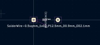
- finally, just click save, and the editor will shut and put you back onto the pcb screen, with the now modified footprint - you can just drop it onto the pcb, and connect it the same as any other part.
(the change to the footprint will only apply to this pcb, not the library footprint it came from).
Finally - don't forget button 'B'...
As I've said a few times now, you need to look at alternative possible 'routes' to solve track crossing problems - rotating parts so you can route 'through' them will help, e.g, your R429, C405, etc. - use the map in post #163 as a guide.
You also seem to still be routing various GND pads - don't forget to press the 'B' key on your keyboard every time you do anything that affects the ground plane - that refills the plane & reconnects all the ground terminals to the ground plane. If you don't do that, you'll end up chasing remnants of the ratsnest for weeks... e.g., the track you've draw between R519 and C424 (delete that track completely, and then press 'B' and you'll see what happens) - I am assuming the plane on the bottom of the pcb has been assigned to the 'GND' net.
There should be only ONE track crossing issue that can't be readily resolved, that does require the use of the wire-link 'jumper' (as discussed in post #154, point (2)) - follow the instructions there to add the jumper to the schematic, and get it onto the pcb screen.
Once it's on the pcb screen you can 'edit the footprint' directly (just off to the side somewhere, so it's not interfering with the rest of the pcb while you work on it) - to give it a suitable size (pad separation), as follows:
- Select it, right click, and open it in the footprint editor

- drag and drop the 3 bits you don't need out of the way (for now)

- now put your mouse cursor on the centre of the number '1' pad - the x,y coordinates at the bottom of the screen should be (0.00, 0.00), now do the same for the centre of pad number '2', that'll be at (x=4.60, y=0.00) - note the 4.60 is the pin (pad) separation distance between '1' and '2' in mm. That's the distance you need to increase - to something like 12.00 - 15.00mm
- select all of pad number '2' (together with the purple rectangular 'courtyard' around it, and drag it all together to the right - until it's centred on coordinates of say x=15.00 y=0.00

- now just drag & drop the other 3 bits back to about the same positions as before (ideally you should also edit the long text entry, from P4.60 to P15.00 - just double click it & edit the text as appropriate)

- finally, just click save, and the editor will shut and put you back onto the pcb screen, with the now modified footprint - you can just drop it onto the pcb, and connect it the same as any other part.
(the change to the footprint will only apply to this pcb, not the library footprint it came from).
Finally - don't forget button 'B'...
I've tried to replicate what you posted. I've started again,and I'll look at all the footprints,but the resistors are already tiny. I did delete the other gnd plane and assigned the blue one,pressed b to fill
Just keep pressing 'B' regularly - ANY pad that's on the GND net will automatically be connected to the ground plane (so it doesn't need ANY track at all). It'll need to be pressed regularly as changes are being made to the pcb...
morning.so i have done all the above and managed to do it without the jumperNot quite sure what you mean by 'manually place by hand' - the tracks should all be routed by hand, except, in this case there is one place where an external wire link has to be added which I was going to come to later (it connects one end of R409 to one end of C424). As far as I can see, that's the only one which should be needed if you've followed the NAD manual routings. You can actually see it on the NAD diagram, and it's the white insulated link in the pcb photo.
View attachment 1401666
View attachment 1401667
A lot of the pcb 'snippet' you just posted looks ok (not all...), but before you go any further maybe you could post a thumbnail of the entire pcb - it'll be easier to see if you're making any general mistakes, that'll be easier to fix now than later.
Two points worth mentioning at this point:
(1) For the various ground connections - we'll add a 'ground plane' to the back of the pcb (so the entire back surface becomes 'ground').
- select the bottom copper layer of the pcb (on the RHS of the pcb screen you have the layers list, just select B.Cu - that just means whatever tools you use now will be used on the bottom copper layer)
- select the 'Add Filled Zone' tool, and then draw a rectangle on the pcb which fills almost the entire surface of the pcb (you click each corner of the rectangle going around, and end up back at the starting point) - it'll look like a blue rectangular outline. That's created a 'zone' on the bottom layer.
- press the letter 'B' - that'll 'fill' the zone with copper. It should add 'hatching' to the rectangular outline
- to view the 'zone', you can use the 2 buttons on the LHS of the screen called 'Draw Zone Fills' or 'Draw Zone Outlines' (just toggle to whichever is needed at the time
- finally, to make the new zone into a 'Ground Plane', 'Left click' any point on the zone outline to highlight it, then 'Right click' and select 'Properties' - you should see 'B.Cu' ticked as the active layer - now select '/GND' from the list of available 'nets' - just leave the rest of the entries on their default settings and click OK. That assigns the zone to be part of the GND net.
- 'Left click' away from the pcb surface (to deselect the zone) and press 'B' again.
Note - All of the component terminals which connect to ground (/GND) are now directly connected to /GND via their solder pads, and a bunch of the ratsnest lines will have disappeared (that's why I said ignore the ground connections before).
Until now, everything you've done will have been on the Front Copper (F.Cu) layer (hopefully), but now there's 2 copper layers, so be sure to always select the layer you want to work on... that will apply to the silkscreen layers as well later.
(2) For the wire link - one of the easiest ways I've found is just to add a 'jumper' to the schematic, as follows:
- insert a 'jumper' between R409 & C424 (you'll find jumpers listed in the components lists) as shown below
- annotate the schematic again (so 'JP1' gets added to the annotations)
- add a 'footprint' for the jumper - I used "Connector_Wire:SolderWire-0.5sqmm_1x02_P4.6mm_D0.9mm_OD2.1mm"
- switch to the pcb screen, and 'update' the pcb for changes to the schematic - so the jumper is added as a new component (it's the 2 square 'terminal pads' in the pcb snippet below, above R409 & C424)
That'll add a 2 terminal 'jumper' to be inserted onto the pcb - it needs to be placed in such a way that one terminal can be directly connected to R409 with a new pcb track, and the other terminal can be directly wired to the appropriate terminal of C424.
Note - You will need to 'edit' the footprint to space the 2 terminals of the jumper further apart (you can see from the footprint name that they're only 4.6mm apart in the std. footprint) - that can be done just on the pcb screen (right click, edit footprint, etc.) and saved without affecting the library footprint. It's a useful exercise in itself, for working with footprints (do it off to the side of the pcb screen to avoid accidentally interferring with the pcb layout).
View attachment 1401692 View attachment 1401693
Just an aside - you can 'toggle' (hide) the various layers on/off as needed, so try toggling the front and back fabrication layers off, it'll be easier to see for routing.
this should be all ok now-i did as you suggested and pressed b at regular intervals.
couldnt remember how you said to remove the text, but for now its looking much better
Last edited:
OK, there's a few problems with those routings, but it's getting there.
I was going to sort the grounds later, but now is probably a good time - go back to the schematic, and just change the 2 "Audio Ground" labels to "GND" labels, save it, then switch to the pcb view and click 'Update PCB from Schematic', and then button 'B' again. That'll combine the grounds (as per the NAD original, and remove the need for ANY traces attached to terminal J7, including the trace you have from J7-R401-R403-C403, that's why I said before to ignore all ground pads.
A few points re. positioning the various tracks (and bear in mind I'm FAR from an expert here...) - Avoid 90 degree angles, and certainly anything >90 degrees (e.g., your 2X tracks by C424 and 1X near C419). Aim to keep all tracks as short as (reasonably) possible, but avoid routing tracks 'tightly' around other non-connected pads (e.g., the track from C423 to J2 going around the C417 pad, or the track from R417 to Q409 going around the R429 pad, etc.), that's not a good idea, and note - there are separation distance 'requirements' which will need to be satisfied before a pcb manufacturer would accept the design, e.g., distances between tracks, pads, etc. (the PCB manufacturer automatically checks all that, and a lot more, from the Gerbers - before an order's accepted).
The original NAD pcb does have a long 'looping' track, connecting the 2 main grounds terminals (J2 & J5 on your pcb). Fortunately, the need for that track is eliiminated by the use of the ground plane. Otherwise, excessively long looping tracks should be avoided, e.g., your track from R409 to C415 (that I guess you used to avoid a 'jumper'....). I've spent plenty of time trying to avoid the need for the jumper, as I suspect NAD did originally... but you'll find it much simpler, and technically better, to use it. It's possible to use the double sided nature of the board, and put tracks on the bottom as well - BUT - I wouldn't do that, it's not necessary, and it disrupts the ground plane unnecessarily. A simple wire jumper as also used by the NAD original is more than sufficient.
The majority of your routings look to be in more or less in the right places, but there's plenty you can do in terms of 'optimising' everything - the NAD layout was a good starting point, but because Kicad only uses staright & 45 degree tracks, there are multiple potential improvements on the exact routings. Try for example: moving Q409 so it's 'under' your R419, and turning it 90 degrees anti-clockwise, then reconnecting it with all new tracks. There's a lot more small improvements once you get the main 'structure' in place (I still see new ones every time I look at it...).
Ive got rid of all the gnd's now, but i dont have any right angles, i let the programme do the work.I personaly think this looks ok now, just a little bit of spacing changes and tidying up.

The one thing i have let to do is the jumper, now when i did as suggested in your other post,i end up with the pins very close together, but i just cant get them to part.
so ive done all you said and i get to this stage

And i tried what you said about editing the footprint, but proberbly didnt fully get what you meant, so is it here you edit?

The one thing i have let to do is the jumper, now when i did as suggested in your other post,i end up with the pins very close together, but i just cant get them to part.
so ive done all you said and i get to this stage
And i tried what you said about editing the footprint, but proberbly didnt fully get what you meant, so is it here you edit?
No - go back to the first image in post #184 (that's what the whole screen should look like when you start editing it).
Once you have the jumper footprint onto the pcb screen (with the pads quite close together), just click on the jumper to highlight it, then right-click to open the list of choices - choose the one marked 'Open in Footprint editor', and follow the rest of the #184 instructions.
Once you have the jumper footprint onto the pcb screen (with the pads quite close together), just click on the jumper to highlight it, then right-click to open the list of choices - choose the one marked 'Open in Footprint editor', and follow the rest of the #184 instructions.
You didn't select it all. Just click the 'undo' button at the top of the page, and try again - or 'drag' the square & circle across to the right, to be centred on the #2 pad. With the way you have it set up, you'll also need to change the pad numbers around - just double-cllick exactly on the '1' and change it to '2', then do the same with the '2', changing it to '1'
Sorry - just noticed your comment about layers - you can turn them 'on' or 'off' in the appearance manager (the Front & Back Adhesive layers in the image below are turned 'off', the others are all 'on').
Those controls just control what's visible and what's being worked on, they don't change anything on the pcb itself, so you can just flick them on/off whenever needed / depending on what you're doing..

Those controls just control what's visible and what's being worked on, they don't change anything on the pcb itself, so you can just flick them on/off whenever needed / depending on what you're doing..

I already posted a 'map' in post # 163, that was produced from the schematic you should have now...
As I've said a few times now, you need to look at alternative possible 'routes' to solve track crossing problems - rotating parts so you can route 'through' them will help, e.g, your R429, C405, etc. - use the map in post #163 as a guide.
You also seem to still be routing various GND pads - don't forget to press the 'B' key on your keyboard every time you do anything that affects the ground plane - that refills the plane & reconnects all the ground terminals to the ground plane. If you don't do that, you'll end up chasing remnants of the ratsnest for weeks... e.g., the track you've draw between R519 and C424 (delete that track completely, and then press 'B' and you'll see what happens) - I am assuming the plane on the bottom of the pcb has been assigned to the 'GND' net.
There should be only ONE track crossing issue that can't be readily resolved, that does require the use of the wire-link 'jumper' (as discussed in post #154, point (2)) - follow the instructions there to add the jumper to the schematic, and get it onto the pcb screen.
Once it's on the pcb screen you can 'edit the footprint' directly (just off to the side somewhere, so it's not interfering with the rest of the pcb while you work on it) - to give it a suitable size (pad separation), as follows:
- Select it, right click, and open it in the footprint editor
View attachment 1404402
- drag and drop the 3 bits you don't need out of the way (for now)
View attachment 1404403
View attachment 1404404
- now put your mouse cursor on the centre of the number '1' pad - the x,y coordinates at the bottom of the screen should be (0.00, 0.00), now do the same for the centre of pad number '2', that'll be at (x=4.60, y=0.00) - note the 4.60 is the pin (pad) separation distance between '1' and '2' in mm. That's the distance you need to increase - to something like 12.00 - 15.00mm
- select all of pad number '2' (together with the purple rectangular 'courtyard' around it, and drag it all together to the right - until it's centred on coordinates of say x=15.00 y=0.00
- now just drag & drop the other 3 bits back to about the same positions as before (ideally you should also edit the long text entry, from P4.60 to P15.00 - just double click it & edit the text as appropriate)
View attachment 1404405
- finally, just click save, and the editor will shut and put you back onto the pcb screen, with the now modified footprint - you can just drop it onto the pcb, and connect it the same as any other part.
(the change to the footprint will only apply to this pcb, not the library footprint it came from).
Finally - don't forget button 'B'...
- select all of pad number '2' (together with the purple rectangular 'courtyard' around it, and drag it all together to the right - until it's centred on coordinates of say x=15.00 y=0.00
When you're on the footprint editor screen - just press and hold the mouse Left button, 'drag' a rectangle around the whole of pad 2, and release the mouse button - that'll select (and highlight) everything inside the rectangle including the pad, the purple square, everything. Then just press and hold the mouse Left button anywhere inside the highlighted area (to select it all) and drag it all together to it's new location - then release the mouse button to 'drop' it there.
tried that, when im in the editor, the purple squares are not thereNot quite sure what you mean by 'manually place by hand' - the tracks should all be routed by hand, except, in this case there is one place where an external wire link has to be added which I was going to come to later (it connects one end of R409 to one end of C424). As far as I can see, that's the only one which should be needed if you've followed the NAD manual routings. You can actually see it on the NAD diagram, and it's the white insulated link in the pcb photo.
View attachment 1401666
View attachment 1401667
A lot of the pcb 'snippet' you just posted looks ok (not all...), but before you go any further maybe you could post a thumbnail of the entire pcb - it'll be easier to see if you're making any general mistakes, that'll be easier to fix now than later.
Two points worth mentioning at this point:
(1) For the various ground connections - we'll add a 'ground plane' to the back of the pcb (so the entire back surface becomes 'ground').
- select the bottom copper layer of the pcb (on the RHS of the pcb screen you have the layers list, just select B.Cu - that just means whatever tools you use now will be used on the bottom copper layer)
- select the 'Add Filled Zone' tool, and then draw a rectangle on the pcb which fills almost the entire surface of the pcb (you click each corner of the rectangle going around, and end up back at the starting point) - it'll look like a blue rectangular outline. That's created a 'zone' on the bottom layer.
- press the letter 'B' - that'll 'fill' the zone with copper. It should add 'hatching' to the rectangular outline
- to view the 'zone', you can use the 2 buttons on the LHS of the screen called 'Draw Zone Fills' or 'Draw Zone Outlines' (just toggle to whichever is needed at the time
- finally, to make the new zone into a 'Ground Plane', 'Left click' any point on the zone outline to highlight it, then 'Right click' and select 'Properties' - you should see 'B.Cu' ticked as the active layer - now select '/GND' from the list of available 'nets' - just leave the rest of the entries on their default settings and click OK. That assigns the zone to be part of the GND net.
- 'Left click' away from the pcb surface (to deselect the zone) and press 'B' again.
Note - All of the component terminals which connect to ground (/GND) are now directly connected to /GND via their solder pads, and a bunch of the ratsnest lines will have disappeared (that's why I said ignore the ground connections before).
Until now, everything you've done will have been on the Front Copper (F.Cu) layer (hopefully), but now there's 2 copper layers, so be sure to always select the layer you want to work on... that will apply to the silkscreen layers as well later.
(2) For the wire link - one of the easiest ways I've found is just to add a 'jumper' to the schematic, as follows:
- insert a 'jumper' between R409 & C424 (you'll find jumpers listed in the components lists) as shown below
- annotate the schematic again (so 'JP1' gets added to the annotations)
- add a 'footprint' for the jumper - I used "Connector_Wire:SolderWire-0.5sqmm_1x02_P4.6mm_D0.9mm_OD2.1mm"
- switch to the pcb screen, and 'update' the pcb for changes to the schematic - so the jumper is added as a new component (it's the 2 square 'terminal pads' in the pcb snippet below, above R409 & C424)
That'll add a 2 terminal 'jumper' to be inserted onto the pcb - it needs to be placed in such a way that one terminal can be directly connected to R409 with a new pcb track, and the other terminal can be directly wired to the appropriate terminal of C424.
Note - You will need to 'edit' the footprint to space the 2 terminals of the jumper further apart (you can see from the footprint name that they're only 4.6mm apart in the std. footprint) - that can be done just on the pcb screen (right click, edit footprint, etc.) and saved without affecting the library footprint. It's a useful exercise in itself, for working with footprints (do it off to the side of the pcb screen to avoid accidentally interferring with the pcb layout).
View attachment 1401692 View attachment 1401693
Just an aside - you can 'toggle' (hide) the various layers on/off as needed, so try toggling the front and back fabrication layers off, it'll be easier to see for routing.
The purple courtyards are there in the original footprint, so you must have deleted them somehow (I've loaded Kicad 8 as well, so it's the same as yours).
Go to your pcb screen, select the jumer footprint and delete it - so it vanishes from the screen entirely.
Then use the 'Tools' menu at the top of the pcb screen, and choose the 'Update pcb from schematic' option - that should add a fresh copy of the footprint to the pcb screen - then you can try it again.
- Home
- Amplifiers
- Solid State
- NAD 3030 complete rebuild
