s
ive been looking at the pcb layout.That looks like quite an involved bit of work.
so i have completed all the above as suggested# The Input, Output, Vcc & Vee labels should all work, as far as I can see, and they all have terminals assigned to them - so J1, J3, J2, J4 resp. - should be all good.
# I've probably confused you with splitting the grounds, that's still causing the same small error below your C423, as well as several others. While splitting them is not absolutely necessary, it does make it a bit easier to layout the pcb to match the NAD original, so try this:
(1) delete the GND label AND the ground symbol below R403, then just draw a wire from the bottom of R403 to connect below R401 (between R401 and your 'Audio Ground' label) - that's all that's needed to connect R403 to the 'Audio Ground' net.
(2) delete the GND label and the ground symbol below C403, and draw a wire from the bottom of C403 to connect to the wire below R403 - that's now connected C403 to the 'Audio Ground' net as well.
(3) delete the GND label and the ground sybol below C417, so there's just a bare wire below C417 - then just attach an 'Audio Ground' label to that bare wire, nothing else (the label name & spelling etc. must be identical to your 'Audio Ground' label below R401. You'll now have R401, R403, C403, and C417 all attached to the same 'Audio Ground' NET - that'll be one of the grounds complete.
Note - there is only one terminal associated with the 'Audio Ground' NET (J7 in your schematic above) - but any part attached to the 'Audio Ground' NET will automatically be attached electrically to the same J7 terminal, e.g., C417 - there's no wire link across to J7, but it has the same NET label, so is 'attached' anyway. It's key to read up on what NETS are and how they're used if you'll be using Kicad (or similar) in future.
(4) For the other ground, the easiest will be to just keep using 'GND' - so the GND symbol & labels below C423 look good, below R419 look good, below C419 look good, and below R433 look good. That means that all those points are correctly attached to the 'GND' NET - BUT - notice, none of them have a terminal associated with them, so there is no 'GND' terminal as such (that's actually why you still have same red arrow error below C423). In fact, you've lost the GND terminal by adding a 'Supply Ground' label. Just delete the 'supply ground' label, and replace it with a GND net label - then you have the GND net correctly tied to the J5 terminal, and the second ground should be (almost) complete.
# The area around R409 & C424 still has errors, not least regarding the neg. (Vee) supply rail, or lack thereof.... check it against the manual schematic, and you should be able to complete the GND net as well.
# R431 also seems to have added an issue now.
That's all I can see at the moment, so it's getting there slowly. The reason I may seem somewhat insistent on getting the schematic correct, is that everything else depends upon it - the 'nets' that are being defined by your schematic are what form the basis of ALL of the pcb track layout, if the nets are wrong, the pcb's wrong.
I'm still using Kicad 6.0, so all track layout is manual. I believe there is an autorouter option for Kicad 8, but I know nothing about it yet, and to be honest it's far more educational to do it manually anyway.
Finally, as an aside - it's simpler if you zip the project files, and just 'post' the zipped file into this thread, e.g., _pro, _sch, _pcb files and the _prl file if there is one. It takes up a lot less forum space, and is much easier to work with.
ive been looking at the pcb layout.That looks like quite an involved bit of work.
Attachments
@poundy - OK, I'm back after 'xmas now, and have pc (& Kicad) access again...
Good to see the schematic progressing: mz543578854 already highlighted the shorted cap - don't forget the missing Vee rail supply and the wrong ground net label (all in my notes above).
The only other errors I can see in the schematic now are various part values, but those shouldn't affect generation of the pcb.
Once the area around R409 / C424 is correct, you'll be able to proceed with sorting the pcb tracks - note - if R409/C424 is not corrected, the netlist & ratsnest (that are generated from the schematic) will both be wrong, and it will 'force' the pcb to be wrong (the netlist & ratsnest essentially define where tracks can / cannot be placed).
I see you've made a good start on arranging the parts on the pcb (as per the NAD original layout), so just a couple of comments that might make things clearer before you start the tracks:
# It's worth remembering that the pcb sheet is now in the 3D world, as opposed to the 2D schematic, so, all the parts are now accurately to scale, to the exact mm dimensions and shapes designated previously via the footprint assignment tool. They also have orientations, so the 2 terminals of e.g., a resistor / capacitor etc., are not the same. Try zooming in on the pads of any part and Kicad will have added 'net labels' (to every pad) that show exactly which 'net' (not part) that particular pad connects to. You may or may not need to rotate parts as you add the tracks.
# Try picking up a couple of parts (one at a time), and just moving them all over the pcb surface (without putting them down) - you should notice the ratsnest 'lines' between the various parts are 'dynamic', e.g., they change according to where the part is... it's not random, but wherever the 'connecting line' jumps to will be in the same 'net'. It'll help when you're laying out the tracks.
# Try selecting the track drawing tool, and then just click on any pad, you'll see several pads become highlighted. Those are all the pads on any particular 'net', that ultimately all need to be connected (electrically). It can be helpful to see where you're trying to go... . Note - you added 'net labels' to the schematic for the 'external' pcb net connections, e.g., Vcc, Vee, GND, etc. Kicad continues to use those, but also automatically generates all of the necessary 'internal' net labels, from the schematic.
# The choices you make for part footprint need to reflect the real world, e.g., not only the physical size of the part, but also the orientation of the part on the board. In the NAD 3030 case for example, a lot of the resistors are vertically mounted, not horizontal. It saves a lot of 'real estate', but does mean you'll probably need to change some of your footprints (there are equivalent vert. & horiz. footprints) in the std libraries, and the orientations NAD used are shown in the service manual diagram. Changing footprints can be done either on the schematic, via the f'ootprint assignment tool (probably the quickest), or directly on the pcb individually (via the edit footprint option) - NOTE - these changes have to be 'mapped' between the schematic & pcb pages, in both cases, e.g., if you change one, the change has to be updated to the other, otherwise it'll all get very confused (use the 'Update pcb from schematic' button, and vice versa...).
Apart from that, probably the easiest is simply to start routing a few tracks and see how it goes... I'd again work to the NAD manual layout as a template (I haven't tried it, but see no reason it won't be close). There is one added 'cheat' they had to make, but you'll probably come across that soon enough, and it's easily sorted then.

Finally - if you start routing the tracks - you can just ignore ALL of the pads directly connected to the Ground or Audio Ground nets, don't bother trying to connect them, it'll be easier and tidier to just add a ground plane later.
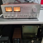
well ive finished the main part of the amp, and it sounds fine.Im pretty pleased how its gone as it looks pretty good compaired to how it was when i first got it, it was ready for the scrap heap.
now onto finishing the pre amp boards
now onto finishing the pre amp boards
Attachments


done, cheers
any idea why i would have these additional pins that are not allocated? should i delete?@poundy - OK, I'm back after 'xmas now, and have pc (& Kicad) access again...
Good to see the schematic progressing: mz543578854 already highlighted the shorted cap - don't forget the missing Vee rail supply and the wrong ground net label (all in my notes above).
The only other errors I can see in the schematic now are various part values, but those shouldn't affect generation of the pcb.
Once the area around R409 / C424 is correct, you'll be able to proceed with sorting the pcb tracks - note - if R409/C424 is not corrected, the netlist & ratsnest (that are generated from the schematic) will both be wrong, and it will 'force' the pcb to be wrong (the netlist & ratsnest essentially define where tracks can / cannot be placed).
I see you've made a good start on arranging the parts on the pcb (as per the NAD original layout), so just a couple of comments that might make things clearer before you start the tracks:
# It's worth remembering that the pcb sheet is now in the 3D world, as opposed to the 2D schematic, so, all the parts are now accurately to scale, to the exact mm dimensions and shapes designated previously via the footprint assignment tool. They also have orientations, so the 2 terminals of e.g., a resistor / capacitor etc., are not the same. Try zooming in on the pads of any part and Kicad will have added 'net labels' (to every pad) that show exactly which 'net' (not part) that particular pad connects to. You may or may not need to rotate parts as you add the tracks.
# Try picking up a couple of parts (one at a time), and just moving them all over the pcb surface (without putting them down) - you should notice the ratsnest 'lines' between the various parts are 'dynamic', e.g., they change according to where the part is... it's not random, but wherever the 'connecting line' jumps to will be in the same 'net'. It'll help when you're laying out the tracks.
# Try selecting the track drawing tool, and then just click on any pad, you'll see several pads become highlighted. Those are all the pads on any particular 'net', that ultimately all need to be connected (electrically). It can be helpful to see where you're trying to go... . Note - you added 'net labels' to the schematic for the 'external' pcb net connections, e.g., Vcc, Vee, GND, etc. Kicad continues to use those, but also automatically generates all of the necessary 'internal' net labels, from the schematic.
# The choices you make for part footprint need to reflect the real world, e.g., not only the physical size of the part, but also the orientation of the part on the board. In the NAD 3030 case for example, a lot of the resistors are vertically mounted, not horizontal. It saves a lot of 'real estate', but does mean you'll probably need to change some of your footprints (there are equivalent vert. & horiz. footprints) in the std libraries, and the orientations NAD used are shown in the service manual diagram. Changing footprints can be done either on the schematic, via the f'ootprint assignment tool (probably the quickest), or directly on the pcb individually (via the edit footprint option) - NOTE - these changes have to be 'mapped' between the schematic & pcb pages, in both cases, e.g., if you change one, the change has to be updated to the other, otherwise it'll all get very confused (use the 'Update pcb from schematic' button, and vice versa...).
Apart from that, probably the easiest is simply to start routing a few tracks and see how it goes... I'd again work to the NAD manual layout as a template (I haven't tried it, but see no reason it won't be close). There is one added 'cheat' they had to make, but you'll probably come across that soon enough, and it's easily sorted then.
They would have been 'transferred' onto the pcb from one of your earlier schematic versions, and I assume subsequently deleted from the schematic but not from the pcb.
You can just select & delete them on the pcb screen.
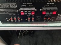
ps - I like the champagne fascia, it suits it well - unusual to see one of those. Mine are both black (amp & tuner).
You can just select & delete them on the pcb screen.
ps - I like the champagne fascia, it suits it well - unusual to see one of those. Mine are both black (amp & tuner).
ok ive deleted.
Now with the tracks, which im not going to start just yet, untill the pcb is 100%, i presume these are the programmes current interpritations of the tracks, and these now have to be drawn on as they need to be in thier final positions.Do i draw onto the board and leave/ignore the rats nest?

Now with the tracks, which im not going to start just yet, untill the pcb is 100%, i presume these are the programmes current interpritations of the tracks, and these now have to be drawn on as they need to be in thier final positions.Do i draw onto the board and leave/ignore the rats nest?
No - the 'lines' you're looking at are showing you the 'nets' (the nets defined by you AND the internal nets assigned by Kicad) that correspond exactly to the schematic. They are not representing tracks.
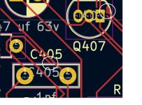
Look at your schematic, say R429 for example - one end of R429 is connected directly (electrically) to R425, C413, and Q407(B), that's one of the internal Kicad assigned 'nets', look at the other end of R429 and that's connected to R427, C415, and Q409(B), that's another of the internal 'nets'. Kicad manages the entire schematic based on the various 'nets' - they are completely defined by the schematic, and cannot be over-ridden on the pcb, e.g., Kicad will not allow you to place tracks which breach the schematic nets (hence the importance of the schematic).
Now look at your pcb screen - select the track routing tool and just click on one of the R429 pads - you should see 4 pads become highlighted, corresponding to the nets just described (zoom in on any of those highlighted pads and they will all have the same net name). The other end of R429 obviously corresponds to the other net. Now if you imagine turning or flipping R429 you can see how that will have a profound impact on how the tracks need to be routed.
Just start down by R401 say and try drawing a few tracks - it'll become clear very quickly, and you can easily delete tracks, re-route them, etc. - you will make a ton of 'mistakes' etc., but they are very quickly and very easily reversed / corrected as you go along. You'll need / want to shuffle the parts around, maybe turn them, etc., one route doesn't work, try another, etc.
Kicad always draws straight lines, vertically, horizontally, or at 45 degrees, and it won't let you cross tracks or connect to the wrong pads.... Here's a couple of tracks I just threw in as an example. Broadly speaking there's no right or wrong, but I'd aim to largely follow the NAD diagram as that's how you've already placed the parts (again, don't worry about any pad that's on a ground net.
@poundy, the "trick" is to position the components so you avoid this. It looks as if you just put them were there was still space on the PCB and now you are trying to just connect them. Especially for a phono stage which is likely prone to catching noise that is not recommended (also not for other layouts).
You should probably get rid of your current tracks, position the parts as in the original and follow how they routed the tracks.
You should probably get rid of your current tracks, position the parts as in the original and follow how they routed the tracks.
Not quite sure what you mean by 'manually place by hand' - the tracks should all be routed by hand, except, in this case there is one place where an external wire link has to be added which I was going to come to later (it connects one end of R409 to one end of C424). As far as I can see, that's the only one which should be needed if you've followed the NAD manual routings. You can actually see it on the NAD diagram, and it's the white insulated link in the pcb photo.


A lot of the pcb 'snippet' you just posted looks ok (not all...), but before you go any further maybe you could post a thumbnail of the entire pcb - it'll be easier to see if you're making any general mistakes, that'll be easier to fix now than later.
Two points worth mentioning at this point:
(1) For the various ground connections - we'll add a 'ground plane' to the back of the pcb (so the entire back surface becomes 'ground').
Note - All of the component terminals which connect to ground (/GND) are now directly connected to /GND via their solder pads, and a bunch of the ratsnest lines will have disappeared (that's why I said ignore the ground connections before).
Until now, everything you've done will have been on the Front Copper (F.Cu) layer (hopefully), but now there's 2 copper layers, so be sure to always select the layer you want to work on... that will apply to the silkscreen layers as well later.
(2) For the wire link - one of the easiest ways I've found is just to add a 'jumper' to the schematic, as follows:
That'll add a 2 terminal 'jumper' to be inserted onto the pcb - it needs to be placed in such a way that one terminal can be directly connected to R409 with a new pcb track, and the other terminal can be directly wired to the appropriate terminal of C424.
Note - You will need to 'edit' the footprint to space the 2 terminals of the jumper further apart (you can see from the footprint name that they're only 4.6mm apart in the std. footprint) - that can be done just on the pcb screen (right click, edit footprint, etc.) and saved without affecting the library footprint. It's a useful exercise in itself, for working with footprints (do it off to the side of the pcb screen to avoid accidentally interferring with the pcb layout).


Just an aside - you can 'toggle' (hide) the various layers on/off as needed, so try toggling the front and back fabrication layers off, it'll be easier to see for routing.
A lot of the pcb 'snippet' you just posted looks ok (not all...), but before you go any further maybe you could post a thumbnail of the entire pcb - it'll be easier to see if you're making any general mistakes, that'll be easier to fix now than later.
Two points worth mentioning at this point:
(1) For the various ground connections - we'll add a 'ground plane' to the back of the pcb (so the entire back surface becomes 'ground').
- select the bottom copper layer of the pcb (on the RHS of the pcb screen you have the layers list, just select B.Cu - that just means whatever tools you use now will be used on the bottom copper layer)
- select the 'Add Filled Zone' tool, and then draw a rectangle on the pcb which fills almost the entire surface of the pcb (you click each corner of the rectangle going around, and end up back at the starting point) - it'll look like a blue rectangular outline. That's created a 'zone' on the bottom layer.
- press the letter 'B' - that'll 'fill' the zone with copper. It should add 'hatching' to the rectangular outline
- to view the 'zone', you can use the 2 buttons on the LHS of the screen called 'Draw Zone Fills' or 'Draw Zone Outlines' (just toggle to whichever is needed at the time
- finally, to make the new zone into a 'Ground Plane', 'Left click' any point on the zone outline to highlight it, then 'Right click' and select 'Properties' - you should see 'B.Cu' ticked as the active layer - now select '/GND' from the list of available 'nets' - just leave the rest of the entries on their default settings and click OK. That assigns the zone to be part of the GND net.
- 'Left click' away from the pcb surface (to deselect the zone) and press 'B' again.
Note - All of the component terminals which connect to ground (/GND) are now directly connected to /GND via their solder pads, and a bunch of the ratsnest lines will have disappeared (that's why I said ignore the ground connections before).
Until now, everything you've done will have been on the Front Copper (F.Cu) layer (hopefully), but now there's 2 copper layers, so be sure to always select the layer you want to work on... that will apply to the silkscreen layers as well later.
(2) For the wire link - one of the easiest ways I've found is just to add a 'jumper' to the schematic, as follows:
- insert a 'jumper' between R409 & C424 (you'll find jumpers listed in the components lists) as shown below
- annotate the schematic again (so 'JP1' gets added to the annotations)
- add a 'footprint' for the jumper - I used "Connector_Wire:SolderWire-0.5sqmm_1x02_P4.6mm_D0.9mm_OD2.1mm"
- switch to the pcb screen, and 'update' the pcb for changes to the schematic - so the jumper is added as a new component (it's the 2 square 'terminal pads' in the pcb snippet below, above R409 & C424)
That'll add a 2 terminal 'jumper' to be inserted onto the pcb - it needs to be placed in such a way that one terminal can be directly connected to R409 with a new pcb track, and the other terminal can be directly wired to the appropriate terminal of C424.
Note - You will need to 'edit' the footprint to space the 2 terminals of the jumper further apart (you can see from the footprint name that they're only 4.6mm apart in the std. footprint) - that can be done just on the pcb screen (right click, edit footprint, etc.) and saved without affecting the library footprint. It's a useful exercise in itself, for working with footprints (do it off to the side of the pcb screen to avoid accidentally interferring with the pcb layout).
Just an aside - you can 'toggle' (hide) the various layers on/off as needed, so try toggling the front and back fabrication layers off, it'll be easier to see for routing.
hi, all of the parts are laid out exactly as they are on the original board.@poundy, the "trick" is to position the components so you avoid this. It looks as if you just put them were there was still space on the PCB and now you are trying to just connect them. Especially for a phono stage which is likely prone to catching noise that is not recommended (also not for other layouts).
You should probably get rid of your current tracks, position the parts as in the original and follow how they routed the tracks.
I see... You should be able to route the tracks according to the original then. Some of your parts are rotated compared to the netlist created fro the schematic (e.g. R407). KiCAD keeps track of all connections and ensures they go to the pin they are connected to in the schematic.
So for some parts like R407, you need to rotate them so the tracks can go the way they are on the original.
It might be easier if you post your KiCAD project and goldie, I or someone else gives you a boost. But of course I do not want to discourage you from learning KiCAD better.
So for some parts like R407, you need to rotate them so the tracks can go the way they are on the original.
It might be easier if you post your KiCAD project and goldie, I or someone else gives you a boost. But of course I do not want to discourage you from learning KiCAD better.
OK - it's worth stopping & reviewing at this point:
You need to look at part orientation and position much more, e.g., look at C401 - if you turn it 90 or 180 degrees you can make the tracks to R401 & R403 much shorter & neater (shorter & neater, is better), and, as 'mz543578854' says, the same for R407... there are quite a few others. You'll need to be critically looking at each component as you add the tracks, what's the best orientation / placement etc. to give the shortest, neatest, track layout... and, as you progress thru' the pcb, you may well need to go back and re-examine parts that you've already done... The original NAD layout & track routings do work and are a very good guide - BUT - they cannot be copied exactly, as Kicad uses straight line tracks, not the 'curvy' tracks of the original. That means slightly re-organising the positions sometimes.
I don't think I can talk you through all the changes... I have been thru' the exercise, and do have a rough 'first pass' layout, so, as 'mz543578854' suggested, maybe the easiest is for you to try to reproduce a picture of that ?
It's not perfect by any means, but it's functional, tidy, and would work (once finished). It should give you plenty of hands-on experience with part & track manipulation if nothing else. It's produced using your earlier posted zip file + my corrections thereof. If your schematic now differs at all, it may not be 100% equivalent, but will be very close provided you corrected your schematic as discussed.
- start by hiding the 'fabrication' layers - so all the white text gets hidden - you don't need to see that info, and it wont appear on the final pcb anyway (in this case).
- you've kept all the horizontal resistor footprints and not used any vertical footprints (as the original does) - that's fine, but it costs 'real estate' on the pcb, so makes routing the tracks more difficult.
- the transistor footprints you chose (with 3 inline terminals) add a little complexity vs. the originals. It's a minor change, but adds a little complexity.
- you've ignored my suggestion to leave the ground cionnections until later - so have added a bunch of un-needed tracks (see my above comments re. adding the ground plane), none of which are needed, and all of which add complexity...
- J1, 2, 3, 4, 5, & 7 are also complicating things - just drag them off the bottom of the pcb for now and don't connect them with tracks yet. The bottom of the pcb shape, and the physical connection to the NAD amp has to be modified later anyway.
- As you're developing the track layout, you also need to bear in mind - every track you add potentially 'blocks' other tracks, e.g., Kicad will not let you cross tracks, as that would violate the electrical rules.
- avoid 90 degree track turns or junctions, use 45 degrees.
You need to look at part orientation and position much more, e.g., look at C401 - if you turn it 90 or 180 degrees you can make the tracks to R401 & R403 much shorter & neater (shorter & neater, is better), and, as 'mz543578854' says, the same for R407... there are quite a few others. You'll need to be critically looking at each component as you add the tracks, what's the best orientation / placement etc. to give the shortest, neatest, track layout... and, as you progress thru' the pcb, you may well need to go back and re-examine parts that you've already done... The original NAD layout & track routings do work and are a very good guide - BUT - they cannot be copied exactly, as Kicad uses straight line tracks, not the 'curvy' tracks of the original. That means slightly re-organising the positions sometimes.
I don't think I can talk you through all the changes... I have been thru' the exercise, and do have a rough 'first pass' layout, so, as 'mz543578854' suggested, maybe the easiest is for you to try to reproduce a picture of that ?
It's not perfect by any means, but it's functional, tidy, and would work (once finished). It should give you plenty of hands-on experience with part & track manipulation if nothing else. It's produced using your earlier posted zip file + my corrections thereof. If your schematic now differs at all, it may not be 100% equivalent, but will be very close provided you corrected your schematic as discussed.
is there a way to get rid of all the tracks and start again as i have messed this one up.In trying to delete tracks ive deleted the component and cant get it back
Ive tried using a back up but they are all read only

Ive tried using a back up but they are all read only
- Home
- Amplifiers
- Solid State
- NAD 3030 complete rebuild