i havent included C 425 or 6-i removed them as you explained in the previous from the last conversations# C425 & C426 are the 1nf ceramic caps on the rear of the phono input sockets - they're not on the phono pcb's. C426 in any case is an 'even' number, so shouldn't be in this channel anyway (all the 'odd' part numbers...). You probably put C426 into the schematic when you were starting, and it got carried over onto the pcb layout (& 3D viewer). At some point after that, you must have deleted it from the schematic, but not 'updated' the pcb layout for changes made to the schematic - so it stayed on the pcb layout. Remember you need to keep the 'schematic information' sychronised with the 'pcb layout information' - changes to one don't necessarily dynamically update to the other (there are contextual buttons on the top menus in Kicad to update one from the other, and vice versa).
Another way to 'find' something like this - is to leave the 'Ratsnest' visible - then you see from the white lines exactly how any part connects into the rest of the circuit. The Ratsnest will become your best friend... I would guess in this case, if you turn it on, C426 will show no connections to anything at all.
# C418 - another 'even' number ? I'd guess it's missing because it's supposed to be missing. Note: there is a slight mistake / inconsistency in the original NAD numbering, with C423 - C426. I'd just keep the odd numbers for this channel.
# Parts layout on the board looks ok for now (vs. the originals). You can just 'put' the J1 to J6 connectors off the bottom of the board for now. If you use the original NAD connection method, you'll need to add the two small board 'extensions' later, where the connections will be made. I'd also aim to try and keep the components all as 'high' up the board as possible. It'll only be a few mm but it'll help prevent 'fouling' of other parts on the main pcb (you can see the available space better than I can, in your rebuilt amp).
# It'll help if you 'label' the Input, Output, and PS 'Nets' on the schematic, one Ground is already done - and I also noticed 2x errors on the schematic, check around your -ve PS rail, and the amp output areas. They need to be corrected before you start laying out pcb tracks, or the errors transfer to the pcb as well.
C418-i noticed that so thats not an issue
The schematic needs to be correct, it drives everything -part numbers & footprints are assigned there, circuit Nets and the Ratsnest are established there.
'Cap Line 1' = is correct for the -ve supply rail to the input.
'Cap Line' with the crossed out wire = I have no idea where the crossed out wire came from, I can't see your pcb layout (e.g., the tracks or Ratsnest). I assume you've added some connections on the pcb layout ? if so, it probably came from an error there. That wire in any case is clearly wrong. C421 at your schematic output is also wrong, it's not connected properly or shorted I can't see clearly, that could have something to do with it too.
'Pre-amp board' = there are 2 Ground connections, one is PS Ground, one is Signal ground.... I mentioned the split grounds several times in earlier posts. They connect to different locations on the NAD main pcb - how much it matters, I don't know, but that's how the original was built. You could certainly modify the circuit so they're the same, but I've not tried that at all.
what i was trying to explain was that on the shot of the pcb itself C419 exists, but it doesn't on the scheme.do i trust the scheme or the PCB shot
on here it exists

On here it doesnt

hence why i drew the line on my scheme

on here it exists
On here it doesnt
hence why i drew the line on my scheme
OK - now I see where you're coming from.
C419 does exist, it's a small 100pf ceramic cap, physically located (on the pcb) underneath C424 (a much larger 1nf ceramic cap) - so it's almost impossible to see with the the boards in the amp. I think the value is 100pf but it's so difficult to see, I can't guarantee it - but the cap IS definitely there.
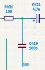
One side of C419 is connected to the +ve of C421, and the other side of it to GND - so, not the wire connection as you've drawn it, but a cap connected from C421(+) to a GND symbol.
Looking at the Ground tracks on the clear pcb image above - both GND connections on the board are indeed connected by a track, which I'd not noticed as 'continuous' before (my apologies). The 2 ends of that track have different connection points from the pcb to the main amp board though (as you've shown in red text), so the easiest is probably still just to use Split Grounds as I suggested before. Alternatively, I assume you could add a second GND terminal pin to a single GND Net, and 'split' the 2 connection points that way. I've never tried it, but I guess it would work.
It'll actually become much easier when you use a GND plane on the bottom of the pcb, then any component connected directly to GND will automatically be connected via the bottom layer of the pcb, and doesn't need any track on the top surface at all. I didn't want to get into that yet, until you'd mastered the basics of getting from the schematic to a pcb and routing the tracks etc. The NAD original pcb layout & routing is in any case set up for a single-sided pcb, with no ground plane.
Your small red arrow fault (in post #122) - will almost certainly disappear once you've got the In, Out, PS Rails, and Gnd (Net) labels sorted correctly.
looks connected ok to me? so im not sure what else to do with this.

'C419 does exist, it's a small 100pf ceramic cap, physically located (on the pcb) underneath C424 (a much larger 1nf ceramic cap) - so it's almost impossible to see with the the boards in the amp. I think the value is 100pf but it's so difficult to see, I can't guarantee it - but the cap IS definitely there'
where abouts is it on the scheme, i cant see it at all??
Your small red arrow fault (in post #122) - will almost certainly disappear once you've got the In, Out, PS Rails, and Gnd (Net) labels sorted correctly.
There's nothing wrong with C423 on your schematic - please read my answer to that Q. at the bottom of post #125 (it's same answer as last time...). I'm fairly sure it's because you have a power supply ground labelled, but no power supply voltage sources... when those are sorted, I suspect it'll vanish.
C419 is shown on the manual pcb drawing (top of your post #124) and in the Service Manual parts list - it is a 100pf/50V ceramic, and is physically present in my own NAD 3030. It is NOT shown on the manual schematic, it was probably added later and someone at NAD forgot to update the schematic.
C419 location is as I described in post #125
C421 itself is still wrong as well - it's not connected (...the open circles), and it's actually shorted (... the wire running connected through it).
Not sure if it's elevant, but one thing when you're working with Kicad - always open the Kicad 'project' file (actually a folder), and then open the schematic and/or pcb files from within the project file. If you open any of the files separately on thee own, without going via the project file, Kicad can lose track of which files below together... and to keep synchronised.
Are the labels different to what I have now ?OK - now I see where you're coming from.
C419 does exist, it's a small 100pf ceramic cap, physically located (on the pcb) underneath C424 (a much larger 1nf ceramic cap) - so it's almost impossible to see with the the boards in the amp. I think the value is 100pf but it's so difficult to see, I can't guarantee it - but the cap IS definitely there.
One side of C419 is connected to the +ve of C421, and the other side of it to GND - so, not the wire connection as you've drawn it, but a cap connected from C421(+) to a GND symbol.
Looking at the Ground tracks on the clear pcb image above - both GND connections on the board are indeed connected by a track, which I'd not noticed as 'continuous' before (my apologies). The 2 ends of that track have different connection points from the pcb to the main amp board though (as you've shown in red text), so the easiest is probably still just to use Split Grounds as I suggested before. Alternatively, I assume you could add a second GND terminal pin to a single GND Net, and 'split' the 2 connection points that way. I've never tried it, but I guess it would work.
It'll actually become much easier when you use a GND plane on the bottom of the pcb, then any component connected directly to GND will automatically be connected via the bottom layer of the pcb, and doesn't need any track on the top surface at all. I didn't want to get into that yet, until you'd mastered the basics of getting from the schematic to a pcb and routing the tracks etc. The NAD original pcb layout & routing is in any case set up for a single-sided pcb, with no ground plane.
Your small red arrow fault (in post #122) - will almost certainly disappear once you've got the In, Out, PS Rails, and Gnd (Net) labels sorted correctly.
I don't know what you have now, but your last post with a full schematic shown was #118 - none of the power rails, or the input or output nets, are labelled on that. The GND net is labelled.
I'm not sure for Kicad 8, but in 6.0 the net label tool is on the right (it's where the add component or add wire tools are) - it looks like a capital 'A' above a line ('Add a Net Label')
I'm not sure for Kicad 8, but in 6.0 the net label tool is on the right (it's where the add component or add wire tools are) - it looks like a capital 'A' above a line ('Add a Net Label')
when you add these labels, are they just dropped next to the item in question? Im just wondering how they end up associated to that position.I don't know what you have now, but your last post with a full schematic shown was #118 - none of the power rails, or the input or output nets, are labelled on that. The GND net is labelled.
I'm not sure for Kicad 8, but in 6.0 the net label tool is on the right (it's where the add component or add wire tools are) - it looks like a capital 'A' above a line ('Add a Net Label')
I just use the 'Add Net Label' button, type the name in ('Vcc' here), and press OK - the symbol on the right then appears (as in the first image below), and can just be dropped onto the schematic wherever it's needed.
The small 'square' has to be dropped onto a wire, so that it connects - it'll disappear once it's connected (as in the second image). As far as I can see, most if not all of your are not connected - you can zoom in to see.
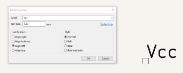
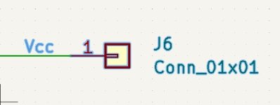
The small 'square' has to be dropped onto a wire, so that it connects - it'll disappear once it's connected (as in the second image). As far as I can see, most if not all of your are not connected - you can zoom in to see.


so ive done as suggested and it appears ok.I just cannot work out whats going on with this one(ground) as ive tried connecting it in all different positionsI just use the 'Add Net Label' button, type the name in ('Vcc' here), and press OK - the symbol on the right then appears (as in the first image below), and can just be dropped onto the schematic wherever it's needed.
The small 'square' has to be dropped onto a wire, so that it connects - it'll disappear once it's connected (as in the second image). As far as I can see, most if not all of your are not connected - you can zoom in to see.
View attachment 1393643
View attachment 1393644
changed the ground as suggested,i didnt notice that one.
looks ok as a pcb though
will the programme route the solder print or does that have to be done manualy
# The Input, Output, Vcc & Vee labels should all work, as far as I can see, and they all have terminals assigned to them - so J1, J3, J2, J4 resp. - should be all good.
# I've probably confused you with splitting the grounds, that's still causing the same small error below your C423, as well as several others. While splitting them is not absolutely necessary, it does make it a bit easier to layout the pcb to match the NAD original, so try this:
(1) delete the GND label AND the ground symbol below R403, then just draw a wire from the bottom of R403 to connect below R401 (between R401 and your 'Audio Ground' label) - that's all that's needed to connect R403 to the 'Audio Ground' net.
(2) delete the GND label and the ground symbol below C403, and draw a wire from the bottom of C403 to connect to the wire below R403 - that's now connected C403 to the 'Audio Ground' net as well.
(3) delete the GND label and the ground sybol below C417, so there's just a bare wire below C417 - then just attach an 'Audio Ground' label to that bare wire, nothing else (the label name & spelling etc. must be identical to your 'Audio Ground' label below R401. You'll now have R401, R403, C403, and C417 all attached to the same 'Audio Ground' NET - that'll be one of the grounds complete.
Note - there is only one terminal associated with the 'Audio Ground' NET (J7 in your schematic above) - but any part attached to the 'Audio Ground' NET will automatically be attached electrically to the same J7 terminal, e.g., C417 - there's no wire link across to J7, but it has the same NET label, so is 'attached' anyway. It's key to read up on what NETS are and how they're used if you'll be using Kicad (or similar) in future.
(4) For the other ground, the easiest will be to just keep using 'GND' - so the GND symbol & labels below C423 look good, below R419 look good, below C419 look good, and below R433 look good. That means that all those points are correctly attached to the 'GND' NET - BUT - notice, none of them have a terminal associated with them, so there is no 'GND' terminal as such (that's actually why you still have same red arrow error below C423). In fact, you've lost the GND terminal by adding a 'Supply Ground' label. Just delete the 'supply ground' label, and replace it with a GND net label - then you have the GND net correctly tied to the J5 terminal, and the second ground should be (almost) complete.
# The area around R409 & C424 still has errors, not least regarding the neg. (Vee) supply rail, or lack thereof.... check it against the manual schematic, and you should be able to complete the GND net as well.
# R431 also seems to have added an issue now.
That's all I can see at the moment, so it's getting there slowly. The reason I may seem somewhat insistent on getting the schematic correct, is that everything else depends upon it - the 'nets' that are being defined by your schematic are what form the basis of ALL of the pcb track layout, if the nets are wrong, the pcb's wrong.
I'm still using Kicad 6.0, so all track layout is manual. I believe there is an autorouter option for Kicad 8, but I know nothing about it yet, and to be honest it's far more educational to do it manually anyway.
Finally, as an aside - it's simpler if you zip the project files, and just 'post' the zipped file into this thread, e.g., _pro, _sch, _pcb files and the _prl file if there is one. It takes up a lot less forum space, and is much easier to work with.
Onl;y just getting back to this now that christmas is done and resolving a few issues with other amps.
@Goldie99 happy christmas by the way.
Ill get on with the instructions from the last post.
I added the rats nest.see what you mean, it will be a bit of work as they are ,or at leats to seem to all be crossing over each other.

@Goldie99 happy christmas by the way.
Ill get on with the instructions from the last post.
I added the rats nest.see what you mean, it will be a bit of work as they are ,or at leats to seem to all be crossing over each other.
- Home
- Amplifiers
- Solid State
- NAD 3030 complete rebuild
 A hell of a task,though,good luck