almost the final version now i noticed i must have at some point deleted C411, now back in place and a few things moved around and tidied up.

That's looking a lot better, but you're missing some tracks - R417 is not connected to Q407/409 at all, R425 is not connected to Vcc, the JP1 pads are not connected to R409 & Vee, others ? The 'ratsnest' should actually be showing you all of those that, have you turned it off ?
Once that'#s sorted, I'd say the next steps should probably be:
After that, it's probably time to start on the board connections at the bottom... but one step at a time. In the mean time, to give you an idea, here's what mine looks like at the moment:

Once that'#s sorted, I'd say the next steps should probably be:
- increase all the track sizes. I've used 0.5mm everywhere intially (see post #172), and then 1.0mm for the power supplies (Vcc & Vee) and the output (from Q407/409(C) onwards. The Vcc, Vee, and output tracks can similarly all be changed via the same main 'Edit' menu - look for changing them one 'net' at a time.
- add the missing board outline (Edge Cuts), and make sure it's < 50mm wide (stick to a rectangular shape for now, but use the 'Graphic Polygon' tool, not the rectangle tool). The height is less critical, but 50 - 60mm should be fine.
- if you want to rotate any of the part designations, e.g., C401, just select the designation text itself (the 'C401') and rotate the same as you would a component. They can obviously be dragged and dropped to wherever you want them.
After that, it's probably time to start on the board connections at the bottom... but one step at a time. In the mean time, to give you an idea, here's what mine looks like at the moment:

ah i must have posted the version before i had finished as i did notice the tracks missing, so had done them 👍
I will look at the other bits later, tracks etc
did we cover the edge cuts before, i dont remember doing those-what are the edge cuts?
I will look at the other bits later, tracks etc
did we cover the edge cuts before, i dont remember doing those-what are the edge cuts?
The 'edge cuts' are literally just that, the edges of the pcb that need to be cut during production - it's the white outline around the outside of your pcb image in post #169, so they were there then... make sure to use the 'Edge cuts' layer, and to draw the outline using the 'Polygon' tool (makes it easier when it comes to adding the 'connection tabs') - use the ruler tool to make sure the mm dimensions are correct.
Kicad is a full professional software package used to make commercial PCBs, so any time you have questions like this, you can almost always just type the question straight into Google and it'll give you the answer... e.g., https://www.google.com/search?q=what+are+edge+cuts+in+Kicad+and+how+do+I+make+them+?
Kicad is a full professional software package used to make commercial PCBs, so any time you have questions like this, you can almost always just type the question straight into Google and it'll give you the answer... e.g., https://www.google.com/search?q=what+are+edge+cuts+in+Kicad+and+how+do+I+make+them+?
so back to this, been busy at work so not had a chance.Ive done the edge cut, now onto the tracks.

This look about right?
This look about right?
Last edited:
The same as when you edited the part reference numbers - 'Edit' - 'Track & Via Properties' - ....
I've set all to 0.5mm, then selectively changed the Vcc, Vee, and Output 'Nets' to 1.0mm
I've set all to 0.5mm, then selectively changed the Vcc, Vee, and Output 'Nets' to 1.0mm
yep worked it out now cheersThe same as when you edited the part reference numbers - 'Edit' - 'Track & Via Properties' - ....
I've set all to 0.5mm, then selectively changed the Vcc, Vee, and Output 'Nets' to 1.0mm
i give up with this.I spend ages rectifying violations, then run the check again and end up with another 132

Try using the 'Update PCB from Schematic' tool (F8), and see what happens, and maybe send me a new copy of the zipped project files.
In the worst case, I have slightly modified pcb's currently being shipped from JLCPCB.
In the worst case, I have slightly modified pcb's currently being shipped from JLCPCB.
Last edited:
This as far as i can see is finished other than one thing that i cant work out in that it is saying.I have the edge cut and i cant see any abnormality with the edge or outline
all of the issues were that it recognised my changed component footprint(where i enlarges pads or holes) so im ignoring those


all of the issues were that it recognised my changed component footprint(where i enlarges pads or holes) so im ignoring those
Let me take a look at the zip file - you shouldn't need to change more than a couple (at most) of the footprints on the pcb screen, the pad & hole sizes of the std f'prints are correct. That is quite likely to cause problems. I think the only f'print I had to change was the jumper.
Note: there's one important aspect we've not covered at all yet, the JLCPCB production 'requirements', e.g., their mechanical production constraints. The pcb has to satisfy those as well, and they dictate track dimensions, clearances between pads tracks, vias, text sizes & thicknesses, etc. etc - those values are what the 'DRC' tool is actually comparing your pcb data to (DRC = Design Rule Constraints). All of the parameters required for the production line equipment are changed on only 1 or 2 screens, so it's far less daunting than it sounds & I can give you a set of values to use & you can see the current Kicad values on the following pages:
FILE - BOARD SET-UP - DESIGN RULES (the JLCPCB values differ only slightly from the Kicad defaults, but will need to be change at some point)
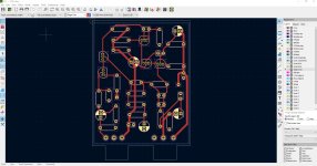
Your snapshot above seems to be showing the 'Edge Cuts' layer (where the cuts will appear in white/grey according to the colour in the small box where it says 'Edge Cuts') - but there's no white/grey edge cuts on the pcb itself. I suspect you may have drawn them on the F.Cu layer instead (the outer 'box' in your image is red).
If it helps at all - this image is essentially correct, albeit with a couple of modifications - the white 'box' around the outside is the edge cuts layer (ignore the marked dimensions, those are only temporary).
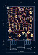

Try this - all I've done is reset all your footpints to the std. library versions (except jumper JP1), you'd somehow changed pads and/or hole sizes for a lot of them, such that they exceded the limits of the purple 'courtyards'. You also had the jumper drawn wrongly on the schematic so it wasn't actually 'jumping' anything, and the pad numbers were reversed - that's all corrected now, in a couple of minutes. I also added the edge-cut, with the dimensions +/- correct along the bottom edge.
I can't enter the DRC constraints for JLCPCB as they need to go directly into your copy of Kicad, but I'll dig them out tomorrow. They might trigger a few more DRC errors, but at the moment the only DRC error showing is the jumper being 'unknown'. Any new ones can be dealt with later anyway. You'll find it gets a lot easier & quicker once you get used to thinking in layers & colours.
You might also find it easier to leave the Layer Appearance Menu / Tool (on the very right of the screen) visible, and just select the appropriate layer to work on there - at the moment it's showing the arrow pointing to the active layer (Edge cuts), and that the colour of items on that layer will be white/grey (every layer has it's own colour). The Front Copper layer is red, the bottom Copper layer is blue, and so all, they all have their own colours.

Attachments
These are the requirements you'll need to use for JLCPCB (other pcb producers are likely to be subtly different) - just copy the screens shown in the pdf file. They may not all be perfect, but they work (for this).
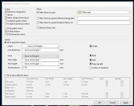
Once those are changed in your Kicad, you'll need to make sure your 'Text' items (e.g., any text on the silkscreen layers, part #'s, etc.) are the correct dimensions - most of your text thicknesses will be wrong. Just use the Edit - 'Text & Graphics Properties' page to correct the thickness value (as per the attached screen) - on any layer with text items showing.
Then check the DRC tool - it probably won't like your C403 reference, just correct that. You also seem to have some 'spurious' (?) R423 text item showing in white/grey on the edge of the pcb - just double click the R423 part symbol (to open it's properties page), tick the 'show' box next to the R423 reference, and OK. That should revert it to yellow text (on the F. Silscreen layer) so you can move it back onto the pcb.
After that, you should only have 1 error showing in the DRC check - for the jumper.... then the fun can start with the connection tabs.
See if you can find how to set the Ground plane 'priority', it may be needed (if you find it, set it to 0).
Once those are changed in your Kicad, you'll need to make sure your 'Text' items (e.g., any text on the silkscreen layers, part #'s, etc.) are the correct dimensions - most of your text thicknesses will be wrong. Just use the Edit - 'Text & Graphics Properties' page to correct the thickness value (as per the attached screen) - on any layer with text items showing.

Then check the DRC tool - it probably won't like your C403 reference, just correct that. You also seem to have some 'spurious' (?) R423 text item showing in white/grey on the edge of the pcb - just double click the R423 part symbol (to open it's properties page), tick the 'show' box next to the R423 reference, and OK. That should revert it to yellow text (on the F. Silscreen layer) so you can move it back onto the pcb.
After that, you should only have 1 error showing in the DRC check - for the jumper.... then the fun can start with the connection tabs.
See if you can find how to set the Ground plane 'priority', it may be needed (if you find it, set it to 0).
Attachments
- Home
- Amplifiers
- Solid State
- NAD 3030 complete rebuild