,my five cents to your kicad project
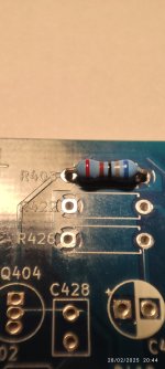
I think you should use resistors with 10.16mm long, if you are using 6.3 mm resistors the 7.62mm seems to be on the short size
In the schematic add the ground symbol.
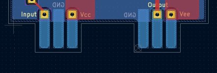
The jumper changed to a 0.1" connector
No big changes of the placement and 2 connections on the ground plane have to be added
Some components change may overcome this
Attachments
does it matter if some of the lines are slightly not entirely straight?
It's probably not visible in the final product, but if you want to do it properly... I'd correct it, if only for the practice.
Click anywhere on the outline of the zone where you have the 'discontinuity', to highlight the zone, then press delete - the zone's gone. Now just redraw a new filled zone on the correct layer (B.Mask in this case, judging from the colour), using a good grid scale (that's why I said before, keep to the one grid scale...), as a simple filled rectangular zone. Don't worry about the size yet. Then, select the outline of the zone (click anywhere on the outline), it should have 8X highlighted points on the outline (the corners and the middle of all sides, only), 'grab' any of the middle points and drag the sides / top / bottom to get the zone size needed.
If you see more than 3 highlighted points on any side - it's not a single line. You can add / remove points on a line, as needed ('create' or 'remove corner'); you need extra to put extra corners in, and so on...
@jpr_pt - welcome on board !
I half agree with you on the resistor sizes; a larger resistor footprint would have been easier for installation, but 7.62mm does work. It's a tight board layout, due to existing width constraints within the NAD 3030 - the pcb can't be wider than ca. 48 - 50 mm. This is what it looks like in reality (courtesy of JLCPCB a few weeks ago).

I'm not sure which ground plane connections & jumper f'print you're referring to - I'm using a different Kicad file at this point. Maybe it would be a good time for a new file update from 'Poundy'. I was going to wait until a final' clean-up' incl. the silks etc., but if there's problems, then now's as good a time as any !
The detailed instructions in Post #224 explain how to connect the pcb 'terminals' to the new zone - just delete the track going to say terminal J1, then drag & drop J1 off to the side somewhere, extend the corresponding zone (+ it's mask zone) upwards several mm, then drag & drop J1 back, on top of the zones. Remember to set the zone priorities, and that you're working on different layers (top, bottom, and mask) for different things... Repeat for the other terminals.
Note - from your image above - you've filled the pcb zones, but none of the connection zones are showing as filled. You still need to assign the zone 'nets' and 'priorities', as explained in the notes (post #224)
ps - I just checked 'jpr_pt's resistor size recommendation - it's straightforward to revise the (horizontal) resistor footprints to the 10.16mm long footprint if you want (change all at one in the footprint assignment tool, then update the pcb for schematic changes), although you would need to tweak / adjust the positions of some of them slightly, and obviously redraw some of the tracks connecting them, but it took me 5 mins to do all of it.
It's probably worth reviewing your component footprints overall - as the importance of component sizes was discussed early on, I've not checked your choices since, but following jpr_pt's comment, I see that your transistor footprints are very small for hand soldering as well, maybe measure one of the TO-92's you'll use for comparison. Again, they are simple to resize if necessary, but beware of inadvertently changing any pinouts.
im hoping this is right now.I scrubbed the others and started again-i am following you instructions.I now have the 6 B.cu layers each with thier assignments -Vcc,Gnd,Vee and the 6 mask layers below.

You were much better off before - now you're just re-doing work you've already done....
On your previous snapshot, where the zones are in place, you could just double click any of the 6 connection zones to open it's properties page, then set its' Net assignment & priority, and close it again - done.
On your previous snapshot, where the zones are in place, you could just double click any of the 6 connection zones to open it's properties page, then set its' Net assignment & priority, and close it again - done.
Good, it seems to be almost there now. Without seeing the full files, I'd say the remaining steps would be:
- connect the J terminals to the 'connection zones' & redo the 4X tracks to them
- check all the component dimensions vs. the parts you'll actually use, correct any footprints as necessary
- re-position / tidy-up the F.Silk layer part references
- double check you've put the JLCPCB constraints into Kicad, run the DRC (Deign Rules Checker), and correct any errors
- plot & zip the Gerber files ready to submit to JLCPCB
Looks about right - I kept the 'terminal' through-holes a few mm higher (so they stay accessible, a bit above the level of the main NAD pcb), but otherwise looks ok.
How does it look in 3D view from the Bottom side ? You might need to change the 'J' solder 'pad connections' to solid from thermal relief - just double click one of the J pads, and check the setting on the 'Connection' tab.
Where you have the B.Mask zones extended down to the bottom 'edge cut' you'll have no solder mask - it won't make much difference, but for correctness you could just pull those zone edges up to match the B.Cu zones.
- Home
- Amplifiers
- Solid State
- NAD 3030 complete rebuild

