Are you saying that since the surface area between the tab and the heat sink is the same, thermal conductance is restricted to the area of the tab for the distance of its thickness, so a thinner tab makes for a shorter constricted area in the thermal path from the die to the heat sink?
You want to get the die as close to the heatsink fins as possible, and use the least amount of thermal paste/copper/alum as possible.
Same goes for computer cpus. There are 2 types, one with a copper heat spreader, and one with an exposed core. The exposed core is better thermally due to one less layer of heatsink compound or epoxy. Alot of heat spreader cpu folk will "lap" down the spreader as thin as possible for better thermal transfer.
A thicker plate means better instantaneous transfer but poorer average transfer. The thicker the plate the longer it takes to get to the fins to dissipate the heat once the heatsink is at operating temp.
Think of it this way. lets say you had 2 heatsinks. One has a really thin base with fins spreading out like a fan at its core. The other heatsink is the same way, only its base is a foot long and insulated. For the first couple of minutes the long base will be cooler due to its huge mass. After both are at operating temp, the thin base is going to dissipate heat faster due to the shorter distance between the fins and the core.
In heat flow, there are many factors that one have to consider.
The but idea here is to remove the heat away from our device rapidly.
The physical size of the tab is fix, yet its thickness has been reduced to better aid the heat flow transfer and its movement away our device.
So yes, a thinner tab does make a smaller constricted area for a thermal path from the die to the heat sink. A thinner tab aids the heat flow transfer base on the TC=25'C conditions, set for the unit. It may not be much, but it helps.
Look at the package. The only real improvement that can be done to the LM317, is to repackage it into a TO218 or 247 package, giving it a larger tab area, as well increase creepage between pins for greater safety.
But a thicker tab will not give it better protection. We want to remove the excess heat, not hold on to it, keeping in the die area.
Take a piece of copper 1/4" thick and draw a line across it, and put it in the freezer.
Take another piece of copper 1/16", draw a line across it, and put it in the freezer. Then after a few hours take them, place them on a stove. And discover which one of the heat flows reach the line first. Just make sure that stove flames are about even.
I am sure the 1/16" piece at 14.7 psi surrounding pressure, will reach the line first. You may be able to see it.
Take Care
Ivey
Thank you Nightpole
The over all goal is to get the heat away, and with surrounding temp. or force air cooling, it will aid it over time. Keeping the unit cooler and reducing failure.
Take Care
Ivey
The over all goal is to get the heat away, and with surrounding temp. or force air cooling, it will aid it over time. Keeping the unit cooler and reducing failure.
Take Care
Ivey
in thermal dynamics, the heat sink tab is a resistance, as is the interface between the heat sink tab and the heat sink (which is usually a much higher resistance). the mass of the heat sink tab and the mass of the heat sink are figured as capacitances. the "charge" on the capacitances is temperature. you can actually model this as an RC circuit in LTSpice. in the following drawing, V1/C1 is the chip itself, R1/C4 is the heatsink tab, R2/C2/R3 is the interface (heatsink insulator, etc...), and C3/R4 is the heat sink. as i said, the capacitances represent mass, and resistances are thermal resistance of the thermal component. the capacitance would be more accurately represented by the specific heat of the material times the mass. the resistances would be in degrees C/Watt.
Attachments

Last edited:
I was sent some JAN2N5303, yesterday.
I was given Saturday's post, and I receive some JAN2N5303. Has anyone used them in a project? I also got some JAN2N3442's as well. A friend of mine in Illinois sent them to me. He is buying surplus auction items.
My friends states that he is getting his information from a person at Big Lots. They buy closeout items. I did not know that. I thought they were like K-Mart.
Take Care
Ivey
in thermal dynamics, the heat sink tab is a resistance, as is the interface between the heat sink tab and the heat sink (which is usually a much higher resistance). the mass of the heat sink tab and the mass of the heat sink are figured as capacitances. the "charge" on the capacitances is temperature. you can actually model this as an RC circuit in LTSpice. in the following drawing, V1/C1 is the chip itself, R1/C4 is the heatsink tab, R2/C2/R3 is the interface (heatsink insulator, etc...), and C3/R4 is the heat sink. as i said, the capacitances represent mass, and resistances are thermal resistance of the thermal component. the capacitance would be more accurately represented by the specific heat of the material times the mass. the resistances would be in degrees C/Watt.
This is all very interesting, but I've been searching the internet and it seems that the price of copper is the main reason for the thinner tabs, and not just with the TO-220 shape.
The thing to look for, I found out, is the term "single gauge". "Dual gauge" packages are of the familiar thickness (1.3-1.5 mm), "single gauge" the thin ones (0.5-0.6 mm).
As I suspected ST and NSC are also going "single gauge". In the newest datasheets, in the mechanical drawings section, the term single gauge is to be found with these brands too now.
I haven't been able to find out if the dual gauge style will disappear or not, but since there seems to be no change or addition in the component identification (e.g. LM317T for the TO-220-shape) to differentiate between the two thicknesses, I'm expecting the worst.
Last edited:
Dual gauge means the lead frame has a varying thickness, single gauge is a level lead frame.
I don't agree, it's either one or the other thickness, but not varying.
Several datasheets mention both the dual gauge as well as the single gauge package seperately. When that is the case, you'll see no variation other than the usual tolerances.
E.g. the most recent datasheet from a L7805 (directly from the ST website) gives the measurements as follows:
Type STD - ST Dual gauge: min. 1.23; max. 1.32 mm
Type STD - ST Single gauge: min. 0.51; max. 0.60 mm
OnSemi, on the other hand doesn't mention the dual gauge in the datasheet but gives a range for the single gauge that obviously also encompasses the dual gauge thickness:
TO-220 Single gauge: min. 0.508; max. 1.39 mm
unfortunately, this smells like an "opportunity" for counterfeiters. if i were the one making the decisions, i would have a date code cutoff from one thickness to the other and leave no ambiguity for someone to exploit.
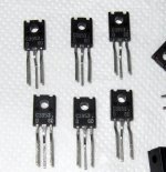
The more shabby Japanese devices look, the bigger chance of being genuine, imo.
So these look fine to me, identical to mine.
Couple of years ago i would have thought chances of Sanyo video TO126s being faked would be relatively small.
Used legs and the correct package details, safer bet than sparkling beauties.
(but what do I know, they shafted me with dual JFETs twice now. my machismo shell may have cracked on the surface only, but my gentle breeze inner nature still feels fragile, soiled and violated)
Thanks. Reassuring. I want them for VAS or cascoding heavy ma and high gm. What do you reckon, good choices?
Eeh, you don't think you'll have to do heavy mA in both cases ?
For lower levels there are both better and cheaper ones.
For lower levels there are both better and cheaper ones.
2sc3953 is good for VAS & Pre-Driver duty.
120Vce0 is a limitation.
It has flat gain from 3mA to 90mA
It has fT~230MHz @7mA
Your Dgrade 60 to 120 hFE @50mA is a bit low but you are never going to use them at that current. Check hFE @ a more usable current for your use.
120Vce0 is a limitation.
It has flat gain from 3mA to 90mA
It has fT~230MHz @7mA
Your Dgrade 60 to 120 hFE @50mA is a bit low but you are never going to use them at that current. Check hFE @ a more usable current for your use.
Thanks Andrew. I can use them at 40-60mA. I have loads of high Idss Jfets 10-15mA that I could group by 4 and shield in a cascode for instance. Do you think its not a good idea when hfe will degrade at about 120?
I did not say degrade. I said Dgrade, The extra letter code shown in your pic.
Dgrade is 60 to 120hFE at test current of 50mA.
Dgrade is 60 to 120hFE at test current of 50mA.
In heat flow, there are many factors that one have to consider.
And one that nobody here had considered yet is R(th)C-S. Yep, case to sink.
The thinner tab will NOT be as flat and have as good a contact if mounted using the scew hole. The thicker tab will have better transfer to the sink in this case. If mounted by pressure contact over the epoxy case (where the actual die is underneath) thermal contact will be similar IF the flatness coming out of the factory is as good (it may not be since they're doing this to be cheap).
If you don't think this matters, try mounting a high power microwave transistor without the proper shims and bang you head for weeks wondering why your gain is 4 dB low.
- Home
- Design & Build
- Parts
- My Transistors, original or copy?