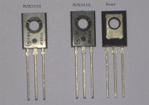
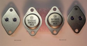
This thread intended to be an information resource for all. Please post measured data and photos for complimentary pairs in one post. The data will be condensed so we have a single post for each type to make things easy to look up. It will be a sticky.
I would like to thank MikeB for encouraging the creation of this resource, and all the members who have collected and posted information previously. Also the members who post new data. We will condense new information into a pre-existing post for the type number. All O.T. posts will be removed to keep this thread clean and useful.
My hope is that this thread will assist members in their semiconductor purchases. Another thread on this can be found here.
-Chris
Mjl4281 / Mjl4302
Data from here:
-Chris
EDIT: Capacitance values are taken from base to emitter with no DC bias, excitation voltage is around 100 mV rms. I normally use 1KHz or 10 KHz.
Thanks to Netlist for pointing this omission out.
Data from here:
I would average these out to 11.5 nF for MJL4281 and 10.9 nF for MJL4302. Anything close (within the tolerance of your own tester) should indicate a real part. The current gain figures would be nice to have. We will add them if they become available.MJL4281
11.45
11.03
11.81
11.07
12.08
MJL4302
10.94
10.95
10.94
10.99
10.92
-Chris
EDIT: Capacitance values are taken from base to emitter with no DC bias, excitation voltage is around 100 mV rms. I normally use 1KHz or 10 KHz.
Thanks to Netlist for pointing this omission out.
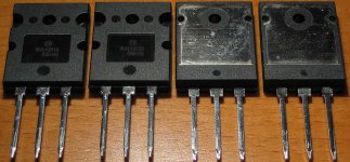
Pictures for MJLs
I will show pictures of MJL0281A/0302A as all MJLs from OnSemi look the same. I found no significant difference to other MJLs.
They should be good as reference to all TO-264 from OnSemi.
These have been aquired through the OnSemi sample program. (Not ROHS conform yet)
Mike
I will show pictures of MJL0281A/0302A as all MJLs from OnSemi look the same. I found no significant difference to other MJLs.
They should be good as reference to all TO-264 from OnSemi.
These have been aquired through the OnSemi sample program. (Not ROHS conform yet)
Mike
Attachments
Mje 15030/15031
Data:
- hfe should be 100 - 150 (20v/50ma)
- capacity (to follow, i have no capacitance meter)
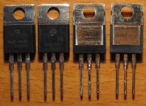
Pictures:
It's likely that all TO220AB cases from OnSemi look the same.
These have been aquired through the OnSemi sample program. (Not ROHS conform yet)
Mike
Data:
- hfe should be 100 - 150 (20v/50ma)
- capacity (to follow, i have no capacitance meter)
Pictures:
It's likely that all TO220AB cases from OnSemi look the same.
These have been aquired through the OnSemi sample program. (Not ROHS conform yet)
Mike
Attachments
Some oldies...
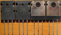
Capacitance measurements for a few classics...these are likely the most counterfeited Japanese transistors around. These are known original Toshiba and NEC devices.
Anyway...
2SB600
1.62nf
1.69nf
1.67nf
1.56nf
1.67nf
1.62nf
2SD555
3.69nf
2.40nf
2.45nf
2.35nf
2.53nf
2.43nf
2SB554
2.27nf
2.20nf
1.95nf
2.55nf
2.26nf
1.95nf
2SD424
2.55nf
2.48nf
2.61nf
2.32nf
2.52nf
2.49nf
Measured with a BK Precision 815 component tester, base-emitter diode reverse-biased
Just for fun, I have some counterfeit 2SD555's and 2SB600's that have not been opened or destroyed.
Counterfeit 2SB600's
1.78nf
1.79nf
1.79nf
1.78nf
Counterfeit 2SD555's
1.26nf
1.28nf
1.29nf
1.25nf
I know for a fact that the ones I tested as good are indeed good, as they are pulls from vintage gear. I also know that the ones I tested as counterfeit are indeed fakes, but I admit that it is annoying that the fake 2SB600's test as close to the original ones as they do...
Excellent thread, BTW...
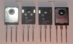
MJW0302A / MJW0281A
Just got some more from a new batch. These are great!
hFE measures just under 100 for all, NPN's maybe one or two counts higher on average.
B-E capacitance is going to average 7.6 nF with the PNP slightly lower by a couple counts (so far).
Here is another picture of both types ......
Just got some more from a new batch. These are great!
hFE measures just under 100 for all, NPN's maybe one or two counts higher on average.
B-E capacitance is going to average 7.6 nF with the PNP slightly lower by a couple counts (so far).
Here is another picture of both types ......
Attachments
MJ15003 / MJ15004
Some more older numbers (brand new stock).
MJ15003G hFE averages 45 ~50, B-E capacitance around 3.65 nF
MJ15004G hFE averages 180 ~190, B-E capacitance around 3.55 nF
I wish the hFE figures were closer between NPN and PNP.
Another mug shot for you .........
Some more older numbers (brand new stock).
MJ15003G hFE averages 45 ~50, B-E capacitance around 3.65 nF
MJ15004G hFE averages 180 ~190, B-E capacitance around 3.55 nF
I wish the hFE figures were closer between NPN and PNP.
Another mug shot for you .........
Attachments
I've a batch of confirmed original MJL4281A, the value is a bit higher compared to the above. It ranges between 12 - 14 nF, avaraging about 13nF.
Mjl21195_mjl21196
Hi all,
I've now measured some new MJL21195 and MJL21196 transistors. PNP and NPN current gains are about 2:1 at low currents. I'm going to have to try this at higher currents.
MJL21195 beta averages about 100 and are very consistent, B-E capacitance is averaging 7.05nF at 10 KHz.
MJL21196 beta ranged from 38 to 62 averaging 52, B-E capacitance varied from 5.02nF to 5.81nF averaging 5.33 nF at the same 10 KHz.
Capacitance meter test voltage was 100 mV AC.
If On Semi could only get the newer devices to be as consistent as the MJW parts, we'd all be in heaven.
-Chris
Attachments
ABOUT TRANSISTOR
Hi, Ladies and Gents:
I want to say a word on transistors, To determine a transistor is not depends on it's b-c, b-e, e-c internal capacitance. When a piece of wafer which is to make transistor, the wafer is about 3 inches in dia. after photo, etching, and layer diffusion, thus many of the transistors were borned.
The point is during diffussion process, the doping in the materials
N or P which N means extra electrons, and P means extra holes.
due to the impurities in these material can come out with different resistance and capacitance. Then with these data to determine the transistor is orginal or false product is not true.
The correct method to determine a transistor is to melt out the casing, ( plastic ) then check under microscope, there would be a lot no. etched on the wafer. this is the only way to identify the transistor. And also consult from the manufacturer about the lot no. and date code.
The date code is eg. 8923, that means this was manufacturer in Yr. 1989, 23 week of that yr.
I'been worked in semicon factory for many yrs. If any Ur question rise, don't hesitate to ask.


WE CONSIDER THE TRUTH OF A MATTER
Hi, Ladies and Gents:
I want to say a word on transistors, To determine a transistor is not depends on it's b-c, b-e, e-c internal capacitance. When a piece of wafer which is to make transistor, the wafer is about 3 inches in dia. after photo, etching, and layer diffusion, thus many of the transistors were borned.
The point is during diffussion process, the doping in the materials
N or P which N means extra electrons, and P means extra holes.
due to the impurities in these material can come out with different resistance and capacitance. Then with these data to determine the transistor is orginal or false product is not true.
The correct method to determine a transistor is to melt out the casing, ( plastic ) then check under microscope, there would be a lot no. etched on the wafer. this is the only way to identify the transistor. And also consult from the manufacturer about the lot no. and date code.
The date code is eg. 8923, that means this was manufacturer in Yr. 1989, 23 week of that yr.
I'been worked in semicon factory for many yrs. If any Ur question rise, don't hesitate to ask.


WE CONSIDER THE TRUTH OF A MATTER
Re: ABOUT TRANSISTOR
Ni Hao!
What everyone hopes for is a simple and non-destructive method of determining fake from genuine transistors, as claimed by its top-mark.
I agree that semiconductor process isn't an exact nor extremely accurate science (I worked at a semicon too, some years ago), thus microprocessors from even the same batch exhibit differences in maximum clock speed.
However, to within a certain 'tolerance' same transistor types will measure the same capacitance, which although partly influenced by impurities etc, will ALL have the same essential geometric properties (i.e. die size, etc), which I *think* has a greater effect on capacitance. And fortunately, the manufacturers of the 'fake' transistors often use dies that are smaller than the originals (we assume, to minimize cost).
The end result is that fake transistor's B-E capacitance is often significantly lower than that of the originals.
OTOH it does seem there are some exceptions... but seems that this is for the significantly older devices... (i.e. 2SB600)
Cheers!
mitwrong said:
due to the impurities in these material can come out with different resistance and capacitance. Then with these data to determine the transistor is orginal or false product is not true.
The correct method to determine a transistor is to melt out the casing, ( plastic ) then check under microscope, there would be a lot no. etched on the wafer. this is the
Ni Hao!
What everyone hopes for is a simple and non-destructive method of determining fake from genuine transistors, as claimed by its top-mark.
I agree that semiconductor process isn't an exact nor extremely accurate science (I worked at a semicon too, some years ago), thus microprocessors from even the same batch exhibit differences in maximum clock speed.
However, to within a certain 'tolerance' same transistor types will measure the same capacitance, which although partly influenced by impurities etc, will ALL have the same essential geometric properties (i.e. die size, etc), which I *think* has a greater effect on capacitance. And fortunately, the manufacturers of the 'fake' transistors often use dies that are smaller than the originals (we assume, to minimize cost).
The end result is that fake transistor's B-E capacitance is often significantly lower than that of the originals.
OTOH it does seem there are some exceptions... but seems that this is for the significantly older devices... (i.e. 2SB600)
Cheers!
re: transistor
to clem_o
Ur info. some are true, some are false.
The false transistor usually they bought the fall out wafer, and do the packing. thus decrease their R&D cost. and not the smaller die to make the tr.
No matter bigger or smaller die, the manufacturing cost almost the same, only the failure rate is diff. the bigger the more, thus due to the diffusion control technique.
with the same diffusion process, the result would have been diff.
It depends on the control of the process, ie: oven temp, turing speed, etching process---- many factor will cause the defects.
may U agree with my opinon?
PS: I am not telling people to destructive, To find out the truth, U may sample size to destruct, this may worthwile in between truth and false. ( sacrface in return of valuable )


WE CONSIDER THE TRUTH, NOTHING BUT THE TRUTH
to clem_o
Ur info. some are true, some are false.
The false transistor usually they bought the fall out wafer, and do the packing. thus decrease their R&D cost. and not the smaller die to make the tr.
No matter bigger or smaller die, the manufacturing cost almost the same, only the failure rate is diff. the bigger the more, thus due to the diffusion control technique.
with the same diffusion process, the result would have been diff.
It depends on the control of the process, ie: oven temp, turing speed, etching process---- many factor will cause the defects.
may U agree with my opinon?
PS: I am not telling people to destructive, To find out the truth, U may sample size to destruct, this may worthwile in between truth and false. ( sacrface in return of valuable )


WE CONSIDER THE TRUTH, NOTHING BUT THE TRUTH
Hi mitwrong,
I normally recommend a visual inspection followed by DC beta and capacitance tests. Not perfect but it should work in most cases. There are always ways to get around the system.
-Chris
I normally recommend a visual inspection followed by DC beta and capacitance tests. Not perfect but it should work in most cases. There are always ways to get around the system.
-Chris
Re: re: transistor
mitwrong,
So they use "reject" dies? Oh my, that's definitely going to be a problem... Thanks for pointing this out as a possibility!
If some of the fakes are actually rejects from the SAME wafer, then wouldn't they have the same batch number anyway?
A question: what are the possible reasons for rejecting at wafer probe? What I can think of:
1. Gross failure (i.e. not at all functional)
2. Low Beta
3. Beta curve out of spec
4. Low ft
Did I miss anything?
Cheers
mitwrong said:
The false transistor usually they bought the fall out wafer, and do the packing. thus decrease their R&D cost. and not the smaller die to make the tr.
mitwrong,
So they use "reject" dies? Oh my, that's definitely going to be a problem... Thanks for pointing this out as a possibility!
If some of the fakes are actually rejects from the SAME wafer, then wouldn't they have the same batch number anyway?
A question: what are the possible reasons for rejecting at wafer probe? What I can think of:
1. Gross failure (i.e. not at all functional)
2. Low Beta
3. Beta curve out of spec
4. Low ft
Did I miss anything?
Cheers
Hi Clem,
Yes.
The expensive part is attaching the die to a casing I would think. I don't see the point of this. Renumbering an existing part bought very cheaply makes far more sense.
Am I on the right track here?
-Chris
Yes.
The expensive part is attaching the die to a casing I would think. I don't see the point of this. Renumbering an existing part bought very cheaply makes far more sense.
Am I on the right track here?
-Chris
Hi Chris,
Good point! Can't verify, either I wasn't listening or they never told me how much die-attach costs... 🙂
Perhaps lump-summing everything into 'packaging' is the easier way to think about it (i.e. epoxy molding, die-attach, wire-bonding, plus the cost of materials - copper base, wire frame, epoxy); how does this compare to the cost of a transistor die???
Cheers
Clem
- Home
- Design & Build
- Parts
- My Transistors, original or copy?
