OK mate, no problem, will pop my head in in the next couple of days. hellabusy at the moment. i'm totally cool with and across the need to have third party testing.
Hi Guys,
Thats a bunch of good work there, I applaud for this great committe work.
Meanwhile, I have found a fairly simple circuit that may further reduce the output noise of a regulator. Its is found here: Shunt circuit using LM833
More testing is found here to indicate the performance of this circuitry: measure power supply noisefloor. The advantage of this circuit is it doesn't really affect the output current of the regulator.
I wonder is it a good integration to the wonderful work done so far?
Last edited:
More testing is found here to indicate the performance of this circuitry: measure power supply noisefloor. The advantage of this circuit is it doesn't really affect the output current of the regulator.
I wonder is it a good integration to the wonderful work done so far?
No, except maybe a pre-reg. All IC regulators are noisy at the HF.
AFAIK also Iko reg is not current-limiting (but it needs to be sized for the allowed current passing through the transistors).
Hi f0, thanks! I was hoping the regulator has low intrinsic noise already and wouldn't need another regulator to clean up things after, like the finesse circuit, which I was familiar with sometime. The noise measurement setup you point to from head-fi is interesting. I had a quick look and didn't see the schematic for the noise amplifier which is the crucial part of the measurement setup and to get that right is not trivial. Here's something that I'd trust:
http://cds.linear.com/docs/Application Note/an124f.pdf
from Jim Williams.
http://cds.linear.com/docs/Application Note/an124f.pdf
from Jim Williams.
fff0, I took the time to look at the detail. Nice thread. I think I should start being active on head-fi 🙂 Indeed, frex has built another of Jim Williams' low noise amps, which is an easier project than the one I was pointing to. I have an e-mu 0404 but I'd rather use my true rms fluke 8920a to measure the noise. One of these days I'll have to build a proper low noise amp too.
No, except maybe a pre-reg. All IC regulators are noisy at the HF.
Unless you are referencing to high frequencies starting from 100khz, else I dont see any further noise measured in there. Maybe a small ferrite bead might help here?
A test
So I run a test on V2. That was a test on a simplistic 36V B+ phono. As far as I know, it it was not tested before for such Vout, the 2N5088 Q1 would not take it, and the 33k R11, R9 would have to change too. I used a BC550C (reversed for pins) for Q1, 68k for R9, R11. Two low Vf red leds also. The input voltage was 43.5V, again something narrow considering the recommendation for more around the mini CCS that biases the first Mosfet. I put an MKT cap for output with a 0.22R resistor in series for chemical cap like losses. I did not have a circa 4uF electrolytic.
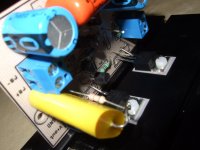
The proto board that I was sent is nice, things fit in place. I would change the proximity of the Mosfets nearer to its edge because it took enough careful manipulation with pliers so they get bended both for the way their legs go and to be in line with the board's edge. Also the input socket has both pins on Vin+, ground has to go to the other side, and I am afraid someone would short the PSU there if not have read some instructions. One connection must be left blank IMO.
I used a 1R in series with Vin to monitor the current draw in mA translated to mV across it. 1k5 5W for dummy load and another DVM on it to monitor Vout. A 4k7 trimmer on long pins initially installed in R2's place. Started it at 500R so to be sure it would start very low for CCS current.
It was a pig to set. I would prefer trimmers for R2,R10 on the final PCB. Around 1k ''R2'' I got 220mA, Vout took time to climb. Current was always drifting slowly for more after the Mosfets got warmer. R10 took some iterations to find with the particular IDSS of J2 and asked Vout. Used a small corrective additional to the main value. Due to the long time for Vout to climb, the input current was reaching an almost alarming value for a little while and drop down when Vout was near its most 3rd. When I took it down to 150mA by using 1k fixed R2 in parallel with 10k, it looked steadier for ICCS. I looked with the scope, did not see oscillation traces with my just 20Mhz scope. That was with or without a 10p NPO comp cap across Q3's C,B. After a while it was steady for heat and readings, I connected the real load. Was OK on it for a while. Went on connecting gear to run FFT. Saw excessive THD upon first run, quickly I checked B+. Had climbed to 40.5V. Shut it down. Next power up, just 5V, smoke, Mosfets went BBQ in a matter of half a second. Grief. It just committed suicide. Left it for next day...
Just 2 Mosfets left don't allow for more smoke luxury. My best guess was a possibly faulty J2. Changed the Mosfets and J2. This time C1 got down to 47uF and the 220uF went to Cout's place. That slow Vout rise must have been the 260uA J201's (J2) current trying to charge the large cap. Might have been faster and safer in 15V regs with 220uF that have been tested by now, but at 36V?
J201 must have had a good discharge on it at a point when with the 220uF... Also the more than likely drift in the CCS when set over 200mA seems it was I did not have enough Vin-Vout around the mini CCS cascode...It worked steady now. The Vout climbed much much faster with the 47uF and the current did not have a chance to shoot up and go down again. I kept it under 150mA and was good for drift. Good news is that the noise floor on FFTs with the phono was the same as with V1.
Listened enough with it. Very good resolution, very good focus, very good tempo. I miss a bit more body and limpness. Maybe its a system thing and its just neutral though. And of course I have to listen more.
So I run a test on V2. That was a test on a simplistic 36V B+ phono. As far as I know, it it was not tested before for such Vout, the 2N5088 Q1 would not take it, and the 33k R11, R9 would have to change too. I used a BC550C (reversed for pins) for Q1, 68k for R9, R11. Two low Vf red leds also. The input voltage was 43.5V, again something narrow considering the recommendation for more around the mini CCS that biases the first Mosfet. I put an MKT cap for output with a 0.22R resistor in series for chemical cap like losses. I did not have a circa 4uF electrolytic.
The proto board that I was sent is nice, things fit in place. I would change the proximity of the Mosfets nearer to its edge because it took enough careful manipulation with pliers so they get bended both for the way their legs go and to be in line with the board's edge. Also the input socket has both pins on Vin+, ground has to go to the other side, and I am afraid someone would short the PSU there if not have read some instructions. One connection must be left blank IMO.
I used a 1R in series with Vin to monitor the current draw in mA translated to mV across it. 1k5 5W for dummy load and another DVM on it to monitor Vout. A 4k7 trimmer on long pins initially installed in R2's place. Started it at 500R so to be sure it would start very low for CCS current.
It was a pig to set. I would prefer trimmers for R2,R10 on the final PCB. Around 1k ''R2'' I got 220mA, Vout took time to climb. Current was always drifting slowly for more after the Mosfets got warmer. R10 took some iterations to find with the particular IDSS of J2 and asked Vout. Used a small corrective additional to the main value. Due to the long time for Vout to climb, the input current was reaching an almost alarming value for a little while and drop down when Vout was near its most 3rd. When I took it down to 150mA by using 1k fixed R2 in parallel with 10k, it looked steadier for ICCS. I looked with the scope, did not see oscillation traces with my just 20Mhz scope. That was with or without a 10p NPO comp cap across Q3's C,B. After a while it was steady for heat and readings, I connected the real load. Was OK on it for a while. Went on connecting gear to run FFT. Saw excessive THD upon first run, quickly I checked B+. Had climbed to 40.5V. Shut it down. Next power up, just 5V, smoke, Mosfets went BBQ in a matter of half a second. Grief. It just committed suicide. Left it for next day...
Just 2 Mosfets left don't allow for more smoke luxury. My best guess was a possibly faulty J2. Changed the Mosfets and J2. This time C1 got down to 47uF and the 220uF went to Cout's place. That slow Vout rise must have been the 260uA J201's (J2) current trying to charge the large cap. Might have been faster and safer in 15V regs with 220uF that have been tested by now, but at 36V?
J201 must have had a good discharge on it at a point when with the 220uF... Also the more than likely drift in the CCS when set over 200mA seems it was I did not have enough Vin-Vout around the mini CCS cascode...It worked steady now. The Vout climbed much much faster with the 47uF and the current did not have a chance to shoot up and go down again. I kept it under 150mA and was good for drift. Good news is that the noise floor on FFTs with the phono was the same as with V1.
Listened enough with it. Very good resolution, very good focus, very good tempo. I miss a bit more body and limpness. Maybe its a system thing and its just neutral though. And of course I have to listen more.
Attachments
Hey guys, I just remembered this, the 2N5210 is a GREAT higher voltage replacement for the 2N5089. LTSpice has a default model for it. I'm thinking it's probably the best replacement.
- keantoken
- keantoken
Thank you Salas, for your thorough report! That temperature induced drift bothered me too, so I fixed it nicely with even more psrr in a new revision which I will post soon. It's not a big change, but I will also redo the PCB layout and run some more tests. I've been running the new revision since yesterday and so far so good, very stable, drift problem fixed too. Will get back with more details later.
kt, it's a good recommendation, thanks!
kt, it's a good recommendation, thanks!
I was luckier! I built it twice without problems. Of course, with mine the output is +/-15V therefore does not have those issues. Also, my Vref cap is only 1.1uF, with 57k total resistance the -3dB point is at 3Hz, a bit high for a full range system but enough for my active 4 way except the woofers.
I did find setting the CCS current very difficult, as I mentioned before. It drifted quite a bit. But with patience, I eventually set it stable.
I did find setting the CCS current very difficult, as I mentioned before. It drifted quite a bit. But with patience, I eventually set it stable.
I haven't been reading this thread for a while so forgive me if this has been raised before but this post & schematic by -ecdesigns- might be of relevance to the current discussions http://www.diyaudio.com/forums/digital-source/140538-lossless-sd-card-player-43.html#post2087091
In it he shows his way of reducing rectifier spikes by using a 3-stage stepped rectifier setup! It might act as another tool in the arsenal of PS taming
In it he shows his way of reducing rectifier spikes by using a 3-stage stepped rectifier setup! It might act as another tool in the arsenal of PS taming
this thread recommends 10V drop across the CCS FET to achieve highest quality sound from the load.
If this 10V is brought about by a 20Vdc supply and a 10Vdc regulated output when mains voltage is at minimum, then expect ~27Vdc supply when mains voltage is at maximum.
The dissipation to be designed for will be 200mA+-10% * 17Vdrop ~3.4W+-10%
If this 10V is brought about by a 20Vdc supply and a 10Vdc regulated output when mains voltage is at minimum, then expect ~27Vdc supply when mains voltage is at maximum.
The dissipation to be designed for will be 200mA+-10% * 17Vdrop ~3.4W+-10%
Thanks Andrew for the analysis.
Then in this case, shouldnt a TO220 heatsink like this be sufficent: TO220 Heatsink ?
Then in this case, shouldnt a TO220 heatsink like this be sufficent: TO220 Heatsink ?
You can not fit 2 side by side. Keep in mind that the Mosfets eye to eye distance is 2.8cm on that proto.
I was talking recently to another member about a high power (4A at 25V) version of the regulator. Perhaps it would be relevant here too.
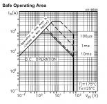
Let's see, 4A at 25V output would mean the shunt mosfet sees the full 25V and has to be able to pass 4A to ground in case the load isn't drawing any power. That would mean the mosfet has to dissipate 100W. First, the mosfet has to be chosen accordingly. Looking at the mosfet description is not enough. For instance the IRFBC40 is rated at 6A and 600V, BUT NOT BOTH AT THE SAME TIME, AND NOT AT ALL TEMPERATURES!!! What we need is to look at the data sheet and find the safe operating area (SOA) graph. Let's make it easy and look at the STW80NF06 mosfet. At first sight you'd think this is overkill, at 60V and 80A rating. But have a look at the attached SOA graph, and follow the DC line. At 25V DC operation seems safe up to about 10A. But, this is at a case temperature of 25C. That's just not going to happen. This thing will get hotter.
So let's look at how to calculate the heat sink thermal resistance, which is what's needed when choosing a heat sink. The formula for calculating the thermal resistance between sink and air is:
theta_sa < (Tj - Ta)/P - (theta_jc + theta_cs)
Where:
* theta_sa = thermal resistance from heat sink to ambient (this is what we want to calculate)
* theta_jc =thermal resistance of mosfet junction to its case, given in the data sheet, for STW80NF06 = 0.5 C/W
* theta_cs = thermal resistance between mosfet case and heat sink, estimated = 0.09 C/W if thermal conductive paste is used and good contact is made
* P = power to dissipate, let's assume 120W
*Tj = max junction temperature for this mosfet = 175 C
*Ta = max ambient temperature, let's estimate = 70 C
If you plug these numbers in the formula you get theta_sa = 0.285 C/W. So the heat sink should have a thermal resistance that is smaller than 0.285 C/W.
How about the IRFBC40 in a to-220 package, with 17V drop at 200mA, or 3.4W dissipation? From the data sheet:
* Tj = 150 C
* theta_jc = 1 C/W
We'll assume the other numbers as before. Then
theta_sa < (150-70)/3.4 - (1 + 0.09) = 22.44 C/W
This means the heat sink that fff0 showed above, rated at 7 C/W, is adequate.
Hope this helps.
Attachments
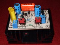
wow.. Salas, is it necssary to use such huge heatsink for 200ma?
Had in mind about 9W in total do dissipate (36Vout) and just had that sink. Its not that big, the board on it on the photo is quite small.
- Status
- Not open for further replies.
- Home
- Amplifiers
- Power Supplies
- My take on a discrete shunt voltage regulator