I underestimate the heat dissipated by a shunt regulator. I suppose the proto board is 3 by 2 inches?Had in mind about 9W in total do dissipate (36Vout) and just had that sink. Its not that big, the board on it on the photo is quite small.
1 more question: Is the calculated wattage applicable to both M1 & M2? Meaning: at any time, both mosfet is going to output around 3.4w(taking Andrew's calculation) and not at 3.4w each, right?
For the CCS Mosfet the dissipation will be any chosen (Vin-Vout)*Iccs. For the shunt Mosfet will be Vout*(Iccs-Iload).
if you want an output of 36Vdc and a CCS current of 200mA, then the minimum input voltage will be 36+10V=46Vdc.
The maximum to minimum voltage range of the mains is ~12%
46 * 1.12 = 51.5 Call it 52Vdc.
The maximum total dissipation is ~52Vdc * 200mA = 10.4W, plus a bit to power the CCS LED string.
The output load + CCS FET + Shunt FET must dissipate all this power.
If the output is shorted the CCS FET has to dissipate 10.4W.
If the output is open circuit then use the formulae that Salas gave.
Thanks Andrew for the in depth explaination.
Is it useful to use the following arrangement: 20Vdc->7815->Iko regulator->5v, adding on the total regulation. Have I missed out any other problem that maybe induced during the process?
Salas, are you able to take any noise figure supression of Iko's regulator?
Is it useful to use the following arrangement: 20Vdc->7815->Iko regulator->5v, adding on the total regulation. Have I missed out any other problem that maybe induced during the process?
Salas, are you able to take any noise figure supression of Iko's regulator?
Last edited:
Beyond a comparison on the total noise floor of the same audio MC Riaa circuit with my V1.0 and Iko's V2.0 5d that I already did and saw no difference, I don't have a better straight way, I lack lab grade equipment and lab methods experience.
revision 5k
Here we go, another update.
I've been very busy running experiments after Salas let me know about his tests. One thing that got to bother me more was the drift of current/voltage with temperature. So I made a minor change to the CCS to make it more stable. While I was at it I also made a change to increase the phase margin to a value which in theory predicts unconditional stability. All this while maintaining good psrr and low output impedance.
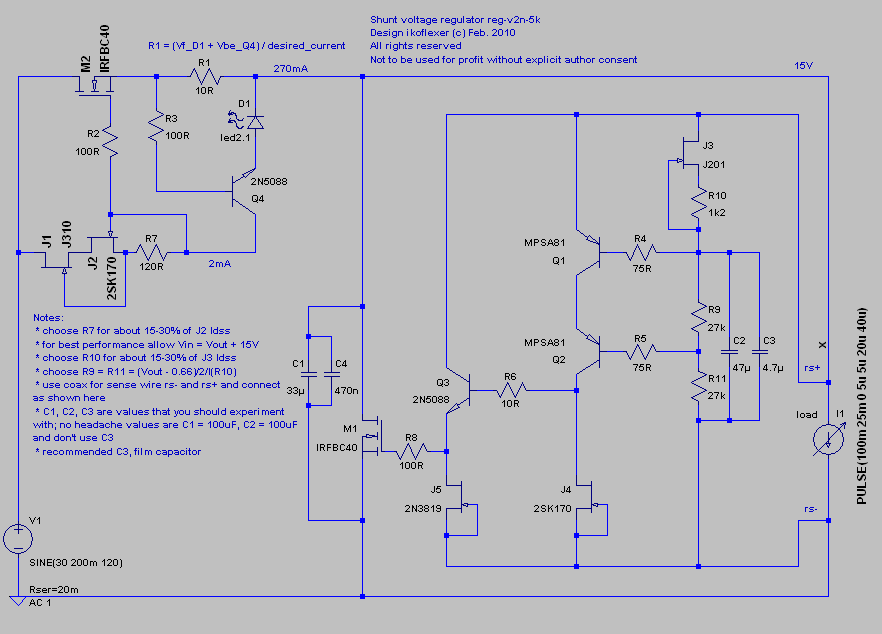
As much as I didn't want to introduce another circuit, especially that I had designed the PCB already, I had to do it, so here it is, below, with some simulated curves. There are more things to say about the circuit, which I'll probably include in the how to document, or answer questions as they come. The output impedance plot changes at low frequency with the value of the Vref bypass capacitor, C2. It's not really practical to have a large value there (the plot shows a 1000uF Zout) because it takes a long time to charge it due to the lowish current that passes through J3. Note the J201 below Q3. One can use other jfets there, 2n3819, 2sk170, etc. It's not a fussy position, but the Idss current is important, so whatever you use to replace J201 make sure Q3 can dissipate the power (voltage across it times Idss). The mini-CCS now employs a J310 on top of the 2sk170, so people won't complain any longer about the proper way of doing it (meaning the top jfet should have higher pinch-off voltage and Idss than the lower mosfet, and the current through should be about 15-30% of Idss).
J4 should have Idss from 6 to 9mA.
Just like before, other mosfets can be used. For higher voltages somethings else should be used for Q3, perhaps a BC550 or equivalent. The way it's presented here should work fine up to 20 something volts out. As for the current limit, it's set via R1. R1 is rougly equal to the sum of the forward voltage of the LED plus the Vbe of Q4, divided by the current limit desired. For very high current loads the circuit needs to be changed a bit, and I'll post later the modifications.
NB: Q1 and Q2 are MPSH81, Q3 and Q4 are 2N5088, M1 and M2 are IRFBC40
I will re-design the PCB as soon as possible if people are still interested.
This circuit was tested in reality for stability and noise for the last few days. The only change is that I've used a 2sk170 for J5 but will test again tonight with a J201, which is easier to find.
Better ripple rejection than before, and increased CCS stability.
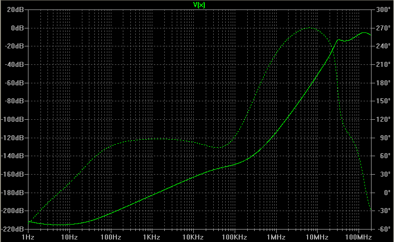
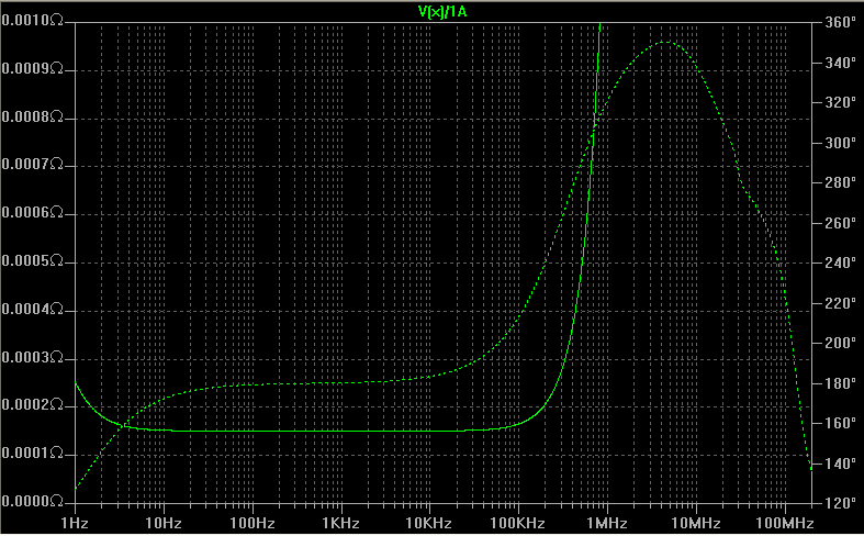
Sub-milliOhm output impedance in the audio range and a bit beyond.
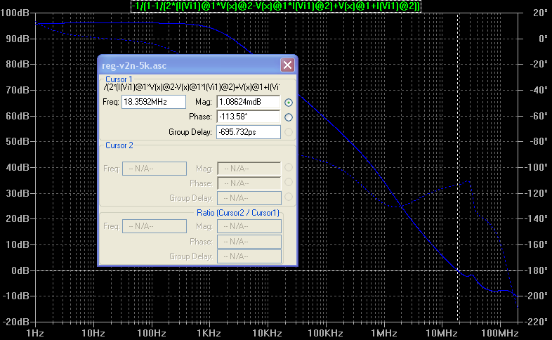
Theoretically the phase margin is about 66 degrees, which should qualify the design as stable. Note that no compensation capacitors are used on the cascode bjts Q1 and Q2.
Here we go, another update.
I've been very busy running experiments after Salas let me know about his tests. One thing that got to bother me more was the drift of current/voltage with temperature. So I made a minor change to the CCS to make it more stable. While I was at it I also made a change to increase the phase margin to a value which in theory predicts unconditional stability. All this while maintaining good psrr and low output impedance.
As much as I didn't want to introduce another circuit, especially that I had designed the PCB already, I had to do it, so here it is, below, with some simulated curves. There are more things to say about the circuit, which I'll probably include in the how to document, or answer questions as they come. The output impedance plot changes at low frequency with the value of the Vref bypass capacitor, C2. It's not really practical to have a large value there (the plot shows a 1000uF Zout) because it takes a long time to charge it due to the lowish current that passes through J3. Note the J201 below Q3. One can use other jfets there, 2n3819, 2sk170, etc. It's not a fussy position, but the Idss current is important, so whatever you use to replace J201 make sure Q3 can dissipate the power (voltage across it times Idss). The mini-CCS now employs a J310 on top of the 2sk170, so people won't complain any longer about the proper way of doing it (meaning the top jfet should have higher pinch-off voltage and Idss than the lower mosfet, and the current through should be about 15-30% of Idss).
J4 should have Idss from 6 to 9mA.
Just like before, other mosfets can be used. For higher voltages somethings else should be used for Q3, perhaps a BC550 or equivalent. The way it's presented here should work fine up to 20 something volts out. As for the current limit, it's set via R1. R1 is rougly equal to the sum of the forward voltage of the LED plus the Vbe of Q4, divided by the current limit desired. For very high current loads the circuit needs to be changed a bit, and I'll post later the modifications.
NB: Q1 and Q2 are MPSH81, Q3 and Q4 are 2N5088, M1 and M2 are IRFBC40
I will re-design the PCB as soon as possible if people are still interested.
This circuit was tested in reality for stability and noise for the last few days. The only change is that I've used a 2sk170 for J5 but will test again tonight with a J201, which is easier to find.
Better ripple rejection than before, and increased CCS stability.
Sub-milliOhm output impedance in the audio range and a bit beyond.
Theoretically the phase margin is about 66 degrees, which should qualify the design as stable. Note that no compensation capacitors are used on the cascode bjts Q1 and Q2.
Last edited:
Here we go, another update.
...
I will re-design the PCB as soon as possible if people are still interested.
Definitely interested.
But please as long as you are changing it, make the new pcb in a way where it is easy to parallel (at least 2) the critical mosfets in high-current applications.
Ikoflexer,
Good one! So Q3 is now connected to the sensor? Negative rail, please.
Regards,
Bill
Good one! So Q3 is now connected to the sensor? Negative rail, please.
Regards,
Bill
Iko, about J5: I think another JFET should be used there as CCS, to allow higher currents to go through Q3. Idss for J201 is max 1 mA
http://www.irf.com/technical-info/appnotes/an-944.pdf
http://www.irf.com/technical-info/appnotes/an-944.pdf
Iko, about J5: I think another JFET should be used there as CCS, to allow higher currents to go through Q3. Idss for J201 is max 1 mA
http://www.irf.com/technical-info/appnotes/an-944.pdf
I had a 2n3819 there, and a 2sk170. But why do you think we should run higher current there?
Edit: I had a comment about this earlier. There is an advantage in running a higher current buffer, but Q3 will have to dissipate some power then, especially at a higher output voltage. A to-92 won't do. But the schematic is not carved in stone, people should definitely experiment with different parts.
Last edited:
He-he, it turns out that Stormsonic is right. So revision 5k was built initially with a 2n3819 for J5, at an Idss of about 6mA. It worked well, so I tested it with a 2sk170 of Idss of about 8mA, not in simulation, but in the real circuit, and it worked well. At the end of the day when I was preparing to post the message I got the "bright" idea to use a J201 for J5, to eliminate the risk of running too much current through the buffer, so that builders would not have one more thing to worry about and calculate. Being late, I tested it only in simulation 🙁 But last night I tested in in the real circuit, and, while it works, my true rms voltmeter showed a slightly larger ripple with J201 than with 2sk170. I'll update the schematic sometime today. Sorry about the confusion.
Definitely interested.
But please as long as you are changing it, make the new pcb in a way where it is easy to parallel (at least 2) the critical mosfets in high-current applications.
😀 that'll be tough, but will try. Maybe one mounted above and one below the board? I'd like to keep the board small (short traces).
Ikoflexer,
Good one! So Q3 is now connected to the sensor? Negative rail, please.
Yes, coming soon, after I get a chance to test it. Should be just a formality anyway. But I can mail you the schematic if you want to run away with it 🙂
Ikoflexer,
Thanks. I am very busy at the moment but if I have good luck I may build your 5k next week. If that happens, I will be naturally your new circuit tester again.
Regards,
Bill
Thanks. I am very busy at the moment but if I have good luck I may build your 5k next week. If that happens, I will be naturally your new circuit tester again.
Regards,
Bill
😀 that'll be tough, but will try. Maybe one mounted above and one below the board?
No, I'd really hope not. It would make pcb mounting very tricky
I'd like to keep the board small (short traces).
I understand this.
No, I'd really hope not. It would make pcb mounting very tricky
I understand this.
not really, I had planned on mounting a series of 'ribs' perpendicular to the chassis and the PCBs can be mounted on their side with the mosfets bent over at right angles, so they are parallel with the PCB surface on either side and each mounted against the rib on either side, rinse and repeat. a number of boards can be mounted this way in a row and still be quite compact.
Modifying the board to accommodate parallel mosfets would involved more room and longer traces for the mosfets. I'm thinking that for higher current applications one cannot avoid very large heat sinks to mount the mosfets on. Then I see no problem using a board as small as this mounted as close as possible to the heat sink, with no mosfets soldered onto the PCB, but with wires leading to the mosfets that are mounted on the heat sink. There would have to be a gate resistor soldered directly to the gate pin of each mosfet, and a small 0R1 resistor of appropriate wattage soldered on the source pin of each shunt mosfet.
I would think this is common practice in power amp mosfet output stages? Has anyone done anything of the sort?
I would think this is common practice in power amp mosfet output stages? Has anyone done anything of the sort?
I would think this is common practice in power amp mosfet output stages? Has anyone done anything of the sort?
That's done with TO-3 packages. Which is less and less used today.
- Status
- Not open for further replies.
- Home
- Amplifiers
- Power Supplies
- My take on a discrete shunt voltage regulator