Simple answer is that they weren't (calculated) but decided on during design/testing as values that worked well under all test conditions (such as squarewave testing and testing into capacitive loads).
Remember that this was all designed many years ago now, long before we were using LTspice and PC's at home.
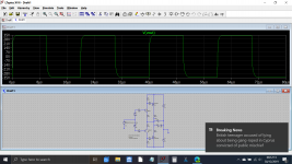
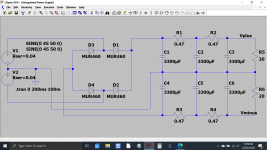
This is the output stage copied in LTspice from the working simulation and shows the output stage in total isolation running open loop, the values used giving a voltage gain of around -1db while maintaining good stability.
Remember that this was all designed many years ago now, long before we were using LTspice and PC's at home.
This is the output stage copied in LTspice from the working simulation and shows the output stage in total isolation running open loop, the values used giving a voltage gain of around -1db while maintaining good stability.
Attachments
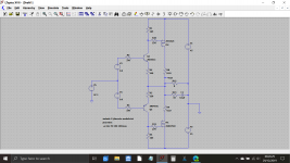
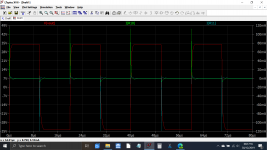
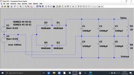
ok, the aspect i'm looking at is the use of a driver stage to provide good drive current for the output FETs, something in the range of 10-15mA
OK, lets take a look at the driver stage again in isolation and see what the current ability is like.
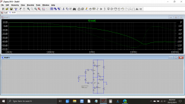
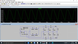
Running the stage at -/+25 volt peak to peak output voltage @ 50kHz shows the output/driver stage is well behaved. The driver currents peak at around -/+110ma.
Now lets replace the FET's with bjt's and slow things down so that we can get more of an idea of sustained currents. The driver currents peak at over 200ma but of more interest is the steady state drive ability which for the bjt's chosen is now over -/+ 50ma.
So within the design goals of the design as whole (an audio amp, not an RF amp 😉) there is no limitation imposed by inadequate driver current.
Attachments

May I please ask if any of you, have a zip with schematic, pcb, component selection (incl. solid relays) and other files?
I have downloaded the zip file from this tread but it do only contain some similar and different schematic.
Mooly did recommend I'd asked here🙂
I have downloaded the zip file from this tread but it do only contain some similar and different schematic.
Mooly did recommend I'd asked here🙂
Question on the CFP output stage
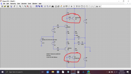
All of the CFP output stages I’ve seen have the emitter from the drivers connected between the source of the output transistors and the output resistors. This amplifier has them connected after the output resistors and adds 220 Ω emitter resistors R19 & R20. Can someone help me understand what this accomplished versus the more traditional CFP circuit?
I’ve done quite a bit of searching on this forum and the web in general and haven’t found any other examples or explanations of this version of the CFP output stage.
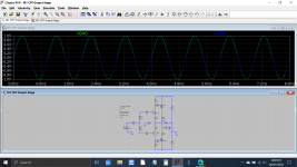
CFP stages can be configured in different ways, for example to give gain as shown here (last image). I went for a unity voltage gain stage (second image). The 220 ohms are a good compromise for driver stability and HF response.
Here is the output stage alone if anyone wants a play.
Here is the output stage alone if anyone wants a play.
Attachments

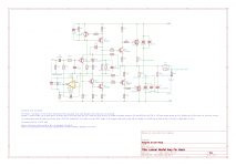
I have made a KiCad schematic of the amplifier and hope it's correct.
Bare in mind that I have about no knowledge about electronic, so please triple check the schematic before using it for anything.
Below an image and the file.
 Moderation Edit... Please see post #991 for updated and corrected version of KiCad file.
My MOSFET amplifier designed for music.
Bare in mind that I have about no knowledge about electronic, so please triple check the schematic before using it for anything.
Below an image and the file.
Moderation Edit... Please see post #991 for updated and corrected version of KiCad file.My MOSFET amplifier designed for music.
Attachments
That looks pretty good  I can only spot one error and that is the opamp inputs are reversed. The + input should be grounded and the 1 meg feeds into the - input.
I can only spot one error and that is the opamp inputs are reversed. The + input should be grounded and the 1 meg feeds into the - input.That looks pretty good
Thanks a lot for checking the schematic, may I please ask you if you can delete the Amp.zip file, so no one risk downloading the wrong schematic?
Here are a picture of what I have now, I hope that it's ok now, so I can upload the finished schematic🙂
Attachments

Last edited:
Power supplies... because someone asked 🙂
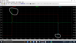
Normally a simple unregulated supply is just fine for designs such as this amplifier. I'm not a big fan of oversized reservoir caps and they can have some disadvantages when the supply is heavily loaded.
Although bigger usually means lower ripple content, it also means the transformer works harder due to the higher peak currents causing resistive losses to be more apparent. In other words the transformer is pushed closer to saturation and it runs hotter.
One thing we can do is add low value resistors as shown here. Its very basic but it does give a worthwhile reduction in ripple amplitude and also it also takes the 'sharp edge' of the ripple waveform making any noise that does get through less intrusive.
My amp uses the simplest of supplies with no resistive filtering.
Look at the scales when comparing these images.
Attachments

What a great and simple design, does not take up much room but since you recommend it, there are no doubt it'll do the job🙂
Thanks 🙂 It does the job just fine. Post #267 here shows the relatively small transformer and reservoir caps I used. I think they were 4700uF from memory.
Output Relays
Output Relays
Thanks 🙂 It does the job just fine. Post #267 here shows the relatively small transformer and reservoir caps I used. I think they were 4700uF from memory.
Output Relays
I'd like how small you've got it, it make et easier to build in🙂
It did all come together well I have to admit. This shows the bridge rectifier bolted to the chassis. There are four 0.1uF caps across each diode in the bridge for suppression.
I would do that differently now and possibly just use a single 0.1uF cap and series resistor of 1 ohm (carbon or metal film) across each secondary.
I would do that differently now and possibly just use a single 0.1uF cap and series resistor of 1 ohm (carbon or metal film) across each secondary.
The schematic shows that C4 and C8 is a 22/50 polystyrene capacitor.
Any recommendation?
Could not find any on DigiKey, where I have found the rest of the components.
Any recommendation?
Could not find any on DigiKey, where I have found the rest of the components.
Which schematic are you looking at? The values for those from the schematic on post #1 don’t match.
Hi and thanks for replying🙂The schematic shows that C4 and C8 is a 22/50 polystyrene capacitor.
Any recommendation?
Could not find any on DigiKey, where I have found the rest of the components.
Sorry forgot to point at the schematic: My MOSFET amplifier designed for music.
It's a KiCad schematic I did draw for all to use🙂
- Home
- Amplifiers
- Solid State
- My MOSFET amplifier designed for music