The delay and protection circuit I used in this amp was a discrete design based on Doug Selfs articles way back in the 1990's in Wireless World magazine. The SSR's I built were a direct swap for the mechanical relays I had used.
You need a simple and reliable switch on delay. There are kits available for this kind of thing or you could try something like this,
http://www.diyaudio.com/forums/solid-state/224957-simple-universal-speaker-delay-using-triac.html
You need a simple and reliable switch on delay. There are kits available for this kind of thing or you could try something like this,
http://www.diyaudio.com/forums/solid-state/224957-simple-universal-speaker-delay-using-triac.html
Hi
I'm confused a bit please someone explain it to me🙂
On the output there is a inductor and with the inductor I see the usually used resistor together (at Alex layout) that not marked at the circuit (usually 2-3W 8R or so that resistor)
I see a 5W extra resistor on the output, what is the function of that, can the inductor be used together with that, I mean winded over the resistor the inductor
If not can I leave out that 0R22 5W resistor and just use the inductor over a 8R 3W resistor
Thank you
Greetings
Attachments
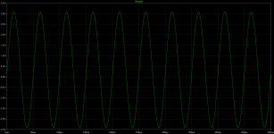
simple but superb
Hi!
no doubt it is simple but genuine design
here is transconductance version
(last time I became a fan of high Zout amps due to their excellent sonics)
with lower gain
and superb performance:
Hi!
no doubt it is simple but genuine design
here is transconductance version
(last time I became a fan of high Zout amps due to their excellent sonics)
with lower gain
and superb performance:
Attachments

Hi
I'm confused a bit please someone explain it to me🙂
On the output there is a inductor and with the inductor I see the usually used resistor together (at Alex layout) that not marked at the circuit (usually 2-3W 8R or so that resistor)
I see a 5W extra resistor on the output, what is the function of that, can the inductor be used together with that, I mean winded over the resistor the inductor
If not can I leave out that 0R22 5W resistor and just use the inductor over a 8R 3W resistor
Thank you
Greetings
Have a read at post #1 and item 1 in the list 🙂 The damping resistor across the coil was not drawn on the original diagrams.
The 0.22 ohm series output resistor is an integral part of the design. It raises the output impedance slightly, and also isolates the amplifier even further from any capacitive loading that may be connected to the output.
Have a read at post #1 and item 1 in the list 🙂 The damping resistor across the coil was not drawn in the original diagrams.
The 0.22 ohm series output resistor is an integral part of the design. It raises the output impedance slightly, and also isolates the amplifier even further from any capacitive loading that may be connected to the output.
Thank you
The reason I asked because Alex did not include at his second layout the coil which is the most important on the output...
Instead 0.22 ohm I use the coil may be the damping resistor
If is OK to ad the 0.22 ohm on the speakers terminal. I have no room on the PC board for the coil and the resistor..
I do like these layout , it would match my heatsink better..
Question
Whit the 2 par power mosfet what would be the acceptable rail voltage. I have a toroid 2X39V that would give about 56VDC rail voltage. If that to much (too high) I have to look for other transformer.. $$$ with shipping cost 😱
Thank you..
Attachments
Last edited:
Karl,
You raise the Zout with the 0.22R resistor and I have also tried this with good result, depending a little on the style of speaker. However, there is another way.......
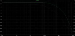
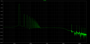
High Loop Gain generates very low Zout and simultaneously improves bandwidth, frequency response, and THD. As long as you control the CLG at the upper pole with correct compensation, the amp will have sufficient phase margin and is therefore quite stable.
It is clear you can decrease loop gain by reducing global feedback. Degeneration, as you know, is one way, but another way is nested feedback, between output of VAS and the inverting node at the first stage. You reduce the global fb by effectively reducing the open loop gain of the gain elements in the amplifier, but we know this increases Zout and increases output stage distortion. But if you have nested fb from VAS to first stage you improve the linearity of these stages, and then use rather less global feedback for the entire amp. Actually you will be reducing the distortion reduction of the output stage alone, since the gain stages will present a more linear signal to the output stage and in this way the cost is not so great as you might expect.
The slowest part of any amp is a common emitter stage, the VAS, so with nested fb you do need to use some lag compensation. What is significant is that the sonic presentation of the amplifier is affected. In fact if you use nested fb from VAS to fb node, and global from output to fb node (the normal way), the global feedback decomposes to the ratio of the output global resistor to the nested resistor. If you use a global divider of 4.7k and 180, you have a closed LG of 27. But if the nested resistor is set at say 100k, the 'open' loop gain of 1st stage to VAS is just 100+0.18/0.18, which is 557, which effectively becomes the open loop gain of the total amp. Thus the ratio of 100k to 4.7k, which is 21.3 (26.6dB) actually becomes the global feedback, and this lower level from your very high level fb then changes the sound of the amp...... try it, you might be surprised!
If you understand all this stuff, please excuse my explanation. But in the rush to achieve very low distortion, it is not intuitive to reduce the global feedback, but it does have ramifications for audio.
Cheers,
Hugh
You raise the Zout with the 0.22R resistor and I have also tried this with good result, depending a little on the style of speaker. However, there is another way.......
High Loop Gain generates very low Zout and simultaneously improves bandwidth, frequency response, and THD. As long as you control the CLG at the upper pole with correct compensation, the amp will have sufficient phase margin and is therefore quite stable.
It is clear you can decrease loop gain by reducing global feedback. Degeneration, as you know, is one way, but another way is nested feedback, between output of VAS and the inverting node at the first stage. You reduce the global fb by effectively reducing the open loop gain of the gain elements in the amplifier, but we know this increases Zout and increases output stage distortion. But if you have nested fb from VAS to first stage you improve the linearity of these stages, and then use rather less global feedback for the entire amp. Actually you will be reducing the distortion reduction of the output stage alone, since the gain stages will present a more linear signal to the output stage and in this way the cost is not so great as you might expect.
The slowest part of any amp is a common emitter stage, the VAS, so with nested fb you do need to use some lag compensation. What is significant is that the sonic presentation of the amplifier is affected. In fact if you use nested fb from VAS to fb node, and global from output to fb node (the normal way), the global feedback decomposes to the ratio of the output global resistor to the nested resistor. If you use a global divider of 4.7k and 180, you have a closed LG of 27. But if the nested resistor is set at say 100k, the 'open' loop gain of 1st stage to VAS is just 100+0.18/0.18, which is 557, which effectively becomes the open loop gain of the total amp. Thus the ratio of 100k to 4.7k, which is 21.3 (26.6dB) actually becomes the global feedback, and this lower level from your very high level fb then changes the sound of the amp...... try it, you might be surprised!
If you understand all this stuff, please excuse my explanation. But in the rush to achieve very low distortion, it is not intuitive to reduce the global feedback, but it does have ramifications for audio.
Cheers,
Hugh
Thank you
The reason I asked because Alex did not include at his second layout the coil which is the most important on the output...
Instead 0.22 ohm I use the coil may be the damping resistor
If is OK to ad the 0.22 ohm on the speakers terminal. I have no room on the PC board for the coil and the resistor..
I do like these layout , it would match my heatsink better..
Question
Whit the 2 par power mosfet what would be the acceptable rail voltage. I have a toroid 2X39V that would give about 56VDC rail voltage. If that to much (too high) I have to look for other transformer.. $$$ with shipping cost 😱
Thank you..
Yes, its perfectly acceptable to add the coil at the speaker terminal of the amp, or you could swap the resistor for the coil on Alex's pcb and add the resistor at the speaker terminal... that's probably the neatest way actually.
56 vdc is too high unless you realise the limitations and are prepared to change the design slightly. The VAS stage and current sink would need TO126 or T0220 style devices to reliably cope with the heat. It may only be 0.5 watt or so but that's above what the 2N5551/5401 can take (unless you can keep them cool... T092 heatsinks are available though). Also, unless you are designing an amp for high voltage output, using unnecessarily high voltage rails simply increases dissipation and actually limits the ability of the amp to drive lower impedance loads safely simply because the outputs are dropping so much voltage. You cross the bounds of the safe operating area of the outputs (SOAR) that much sooner. That applies to any fixed rail design.
Hi Hugh,
Yes I think I follow what you are saying in suggesting to 'wrap' more feedback around the VAS to linearize that stage more, and as a by product it reducing the open loop gain of the amp. That must alter the sonics.
Certainly interesting avenues to explore in future though.
Thanks 🙂
Yes I think I follow what you are saying in suggesting to 'wrap' more feedback around the VAS to linearize that stage more, and as a by product it reducing the open loop gain of the amp. That must alter the sonics.
Certainly interesting avenues to explore in future though.
Thanks 🙂
Yes, its perfectly acceptable to add the coil at the speaker terminal of the amp, or you could swap the resistor for the coil on Alex's pcb and add the resistor at the speaker terminal... that's probably the neatest way actually.
56 vdc is too high unless you realise the limitations and are prepared to change the design slightly. The VAS stage and current sink would need TO126 or T0220 style devices to reliably cope with the heat. It may only be 0.5 watt or so but that's above what the 2N5551/5401 can take (unless you can keep them cool... T092 heatsinks are available though). Also, unless you are designing an amp for high voltage output, using unnecessarily high voltage rails simply increases dissipation and actually limits the ability of the amp to drive lower impedance loads safely simply because the outputs are dropping so much voltage. You cross the bounds of the safe operating area of the outputs (SOAR) that much sooner. That applies to any fixed rail design.
Thank you Mooly
Very detailed, easily understandable answer!
I will try to find (buy) the right V rating transformer.. I do found in my box a very nice 430VA toroid with 2x35V sec. that would be about 49VDC I guess that to too high also. I will drive a 8 ohm speakers.
Other option would be to regulate the PS to drop the voltage but I'm not a big fan of the regulated PS.
I can use a flag style heatsink on the VAS or even bigger something if that make it safe. Other transformer I have it would give below 40VDC about 36- 37VDC or so rail voltage. And only 230VA. I guess to weak for two channel..
What will be the acceptable transformer VA rating, 300VA would be enough for the two channel.
Thank you for your help.
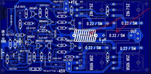
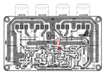
Here is the final layout based on the Alex second design, Thank you Alex! I did mode it by me to feet my heatsink
I will start to collect the parts to the amplifier

Greetings
Attachments
A 230va (so 4.6 amp per winding) 25-0-25 vac toroid would make a very nice amplifier actually. The voltage is always a bit higher anyway at light loading because the transformer voltage is specified at full load, so probably closer to 27-0-27 for much of the time.
In post 531 the layout of the pcb for the amplifier of Mooly is attached. Thanks. it would be helpful to add the dimensions (preferably in mm), so it can be printed on the right scale. Did I miss a post on this? If not, can someone please add the right dimensions?
When someone is planning to make pcb's, or have them made,I would be interested in a pair.
When someone is planning to make pcb's, or have them made,I would be interested in a pair.
In post 531 the layout of the pcb for the amplifier of Mooly is attached. Thanks. it would be helpful to add the dimensions (preferably in mm), so it can be printed on the right scale. Did I miss a post on this? If not, can someone please add the right dimensions?
When someone is planning to make pcb's, or have them made,I would be interested in a pair.
Hello,
I can take a lead in pcb making if sufficient interest is there and alexmm posts gerbers. I am talking bout the layout by alexmm as referenced in Post #1.
octave1audio
In post 531 the layout of the pcb for the amplifier of Mooly is attached. Thanks. it would be helpful to add the dimensions (preferably in mm), so it can be printed on the right scale. Did I miss a post on this? If not, can someone please add the right dimensions?
When someone is planning to make pcb's, or have them made,I would be interested in a pair.
Hello
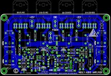
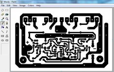
That layout based on Alex design. I only mod it to feet my heat sink an my ideas. Also to make it more iron transfer friendly.
I use paint program on my computer to draw or rework layouts.
The PC board size same wide how Alex made it, I did not touched that dimension.
Usually I try to make my layout a bit larger because I use PRP exotic resistors 9 or 10mm size and caps to. 125-130mm wide will give you the right size. You can scaled it to the right size..
I use pain from Windows XP for that to. Some printer also aloud to scale it to the right size..
Only one part has to be close to feet the chip. The other components lead can be adjusted.
I always draw my layout these way, I own Sprint 6 but so many years I'm doing these way to me now easier than to learn how to use Sprint program. I do not plan to do much layout so I'm sure I do not learn that.
I cant not provide silk screen but you can use Alex artwork or parts location to make your life easier if you choose these layout. Some small change only..
These is the final layout! I hope it helps, I do not want to create confusion. You can always use the Alex design, he did awesome job and has two different type... Just in case if you afraid to use mine.. Also I'm willing to help in case,
Thank you, and thank you Mooly!
Attachments

Last edited:
Mooly I think I will try to replace 2n5551 VAS With Hitachi 2SD667A or ZTX752.
Of course after I build one side with the orig. With the right rail voltage..
The other side I use one of the mentioned transistor for VAS. So I can make A/B test.
I know it has different pin out but I will pay att.
One has 1W disp. the other 0.9W. 2N5551 has 0.5..
I do want to use my 35-0-35V transformer. I have that I would love to use it..
Can you take a look at the data please, thank you
ZTX753 PDF Datasheet - DIODES Incorporated - Datasheets360.com
http://www.redrok.com/NPN_2SD667_80V_1.0A_0.9W_Hfe160_TO-92MOD.pdf
Greetings
The 2SD667A is only 100 volts Vce, the ZTX752 only 80 volts. That's not enough for safety as each transistor sees almost the full combined rail voltage as the output swings toward each rail. You could easily enter a secondary breakdown mode using those.
If you want to go with a 35 volt tranny then try something like the MJE350 for the current source and a modern MJE340 from someone like Fairchild or On-Semi for the VAS.
If you want to go with a 35 volt tranny then try something like the MJE350 for the current source and a modern MJE340 from someone like Fairchild or On-Semi for the VAS.
Hello
That layout based on Alex design. I only mod it to feet my heat sink an my ideas. Also to make it more iron transfer friendly.
I use paint program on my computer to draw or rework layouts.
The PC board size same wide how Alex made it, I did not touched that dimension.
Usually I try to make my layout a bit larger because I use PRP exotic resistors 9 or 10mm size and caps to. 125-130mm wide will give you the right size. You can scaled it to the right size..
I use pain from Windows XP for that to. Some printer also aloud to scale it to the right size..
Only one part has to be close to feet the chip. The other components lead can be adjusted.
I always draw my layout these way, I own Sprint 6 but so many years I'm doing these way to me now easier than to learn how to use Sprint program. I do not plan to do much layout so I'm sure I do not learn that.
I cant not provide silk screen but you can use Alex artwork or parts location to make your life easier if you choose these layout. Some small change only..
These is the final layout! I hope it helps, I do not want to create confusion. You can always use the Alex design, he did awesome job and has two different type... Just in case if you afraid to use mine.. Also I'm willing to help in case,
Thank you, and thank you Mooly!
Stop!. Beware... this version of PCB has an error that was never corrected. Its regarding R10 connected to gnd. it should be to -ve rail as pointed by some gentleman...
Stop!. Beware... this version of PCB has an error that was never corrected. Its regarding R10 connected to gnd. it should be to -ve rail as pointed by some gentleman...
Hi
Thank you
I will go over and check for errors... Thank you for the warning, I thought that was a proven built PC board or layout.
It will take some time but I will correct the error.
Mooly at first I will build it with the recommended rail voltage (I have a transformer but the VA rating only enough for one channel)
After I will try the higher voltage that will be max 49V rail volt..
The 100V transistor should work in these case but that was just an example..
I do have some other higher voltage transistor in TO126 case..
Thanks for the warning🙂
Greetings gabor
- Home
- Amplifiers
- Solid State
- My MOSFET amplifier designed for music