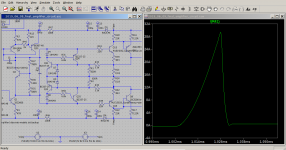
The attachment is an LTSpice screenshot showing the short current spikes with a 1000Hz input signal. The amplifier schematic has been enlarged to clearly show the output short ciruit current limiter, so that, users can make their evaluations, and if they want, comment.
The almost perfect +/-35A peaked short circuit current squarewave has been greatly weakened, and transformed into triangular spikes with a base of 28 microseconds. Their peak is the protection circuit's activation current, which is 29.5A.
The reason for such a high activation current, is to allow for high power bass at full power with a 2 Ohm load.
The protection circuit works on the principle of forcefully latching itself on when the activation threshold voltage is sensed. The circuit remains on until it is de-energized at the succeeding crossover.
Attachments
The distortion gets lower.
Adding two 68kOhm resistors to the output overcurrent protection circuit reduced the distortion figure. I am posting as it would be very interesting to understand why two humble 68kOhm resistors improved the distortion figure.
The added resistors were added in parallel with the signal diodes that are connected to the collectors of the protector circuit.
At 8 Ohms, 141W, the distortion is 0.005%.
At 4 Ohms, 283W, the distortion is 0.007%
At 2 Ohms, 572W, the distortion is 0.017%
The schematic is attached.
Attachments
By preventing Q24 and Q25 from turning on too early? Tried taking those 68k resistors to the rails?
Tried changing D4 and D8 to schottky and losing Q24/Q25? Keep the 68k resistors to the rails. Here the resistors prevent the diodes switching on too early - the 68k can be reduced perhaps to 10k or 22k
Tried changing D4 and D8 to schottky and losing Q24/Q25? Keep the 68k resistors to the rails. Here the resistors prevent the diodes switching on too early - the 68k can be reduced perhaps to 10k or 22k
Some years ago in 2004 Silicon Chip an Australian magazine published articles for a high power amplifier with 4 sets of output power transistors (8 in total). This ran from +/- 70 volt supplies where the protection was a pair of 5A slow blow fuses in the rails.
The distortion at 1kHz measured with Audio Precision test gear was around 0.002% up to 180W into 8 Ohms. This was rated for 200W into that load and 350W into 4 Ohms at 0.1% sinking to 0.0045% at around 280W output.
In contrast to the types used in this circuit the output devices were MJL21193 and MJL21194, the drivers being MJE15030 and MJE15031 in a normal Darlington configuration with emitter resistors set at 0.47R the value determined to provide equal current sharing among the output devices.
The supply rails were decoupled on the pcb close to the output devices by 470uF capacitors. The main supply capacitors included 1W 15k resistors to discharge the capacitors after switch off.
The layout of the pcb and earthing were critical to achieving these results and the board would not fit inside the Wharfedale chassis however the layout does include distortion cancellation features due to the routing of paths in consideration of radiated fields.
The articles show plots of the output stage survival capability with various loads however should a fuse blow it is essential to include a dc protection circuit to disconnect the output terminal from the load.
Somewhere in one of my notebooks I have the formulae for the protection devised by Bailey in the 1960's when power transistors were less robust than ones available now. Devising a layout without these will be an easier task with no fiddling of resistor values.
The routing of the small signal earth shown in the last simulation may be for reasons of drafting convenience. To avoid compromised results it needs to be reviewed for an actual build to follow best practice.
I can provide more detail on this circuit by email request.
Q24 and Q25 prevent the output transistors from damaging heat dissipation in the event of the output being short-circuited. Without them, the output current waveform is a square wave with a peak of 35A which is far too high. The output overcurrent protector circuit works closely like a Schmitt Trigger. Once the tripping threshold is reached, it is turned on and remains on until the voltage reaches crossover. While the output protector is latched on, the output cannot conduct much current.
I asked for comments as I did not expect the distortion figure to be improved with this addition.
Post 541 has a screenshot of the short circuit output current waveform. As you can see, the power dissipation is greatly reduced.
I asked for comments as I did not expect the distortion figure to be improved with this addition.
Post 541 has a screenshot of the short circuit output current waveform. As you can see, the power dissipation is greatly reduced.
No, Q21 and Q22 switch off the drive on overload, Q24 and Q25 just short out the forward voltage of the diodes in order that Q21 and Q22 can function into a CFP output stage where the driver bases are only 0.7V above/below the output rail. Using schottky diodes means there is no need for Q24/Q25's auxiliary function.
With silicon diodes Q21/Q22 can only pull the driver bases to within 0.8V or so of the output, not enough without help. Schottky diodes are one solution, helper transistors Q24/Q25 are another.
With an EF output stage the driver bases are larger and this isn't an issue.
With silicon diodes Q21/Q22 can only pull the driver bases to within 0.8V or so of the output, not enough without help. Schottky diodes are one solution, helper transistors Q24/Q25 are another.
With an EF output stage the driver bases are larger and this isn't an issue.
Last edited:
Having said that surely the collectors of Q24/25 should go to the output rail anyway??? Are they doing anything in that circuit?
Re:- Majona My own work and the execllent work published by Douglas Self confirms the critical importance of layout and earthing in audio amp design. I agree with what you say.
Q24 and Q25 prevent the output transistors from damaging heat dissipation in the event of the output being short-circuited. Without them, the output current waveform is a square wave with a peak of 35A which is far too high. The output overcurrent protector circuit works closely like a Schmitt Trigger. Once the tripping threshold is reached, it is turned on and remains on until the voltage reaches crossover. While the output protector is latched on, the output cannot conduct much current.
I asked for comments as I did not expect the distortion figure to be improved with this addition.
Post 541 has a screenshot of the short circuit output current waveform. As you can see, the power dissipation is greatly reduced.
I looked at this issue from the viewpoint of your having to design a pcb with a lot of elements - in a small space without that skill you will be lucky to do a decent enough job.
The suggestion to use fuses was made to ease pcb congestion and on your previously stated basis of domestic use.
Your output stage should be able to handle a 2R load without failing with 5A slow-blow fuses in the supplies.
It might take 1 second for these to blow under load. That is long enough to deliver peak currents for high power domestic audio.
It appears you are now wanting this as part of a professional entertainment system for continuous high power output. It seems this is more about demonstrating specifications than being objective and practical.
Ah sorry, I misunderstood their purpose, they latch the protection on (as well as reducing the voltage across the diodes). Which is doubly useful.Having said that surely the collectors of Q24/25 should go to the output rail anyway??? Are they doing anything in that circuit?
Here, that business sector is highly competitive and I am not in it. Anyone in it will certainly seek to get the most reputable and expensive products. I purchased a Wharfedale amplifier for the fact, these amplifiers have a flat frequency response, and the price of the S1500 was comfortably within my spending power.mjona said:It appears you are now wanting this as part of a professional entertainment system for continuous high power output. It seems this is more about demonstrating specifications than being objective and practical.
As it is, the amplifier can be used, but I must always make sure the outputs are not shorted, and the 2 Ohm minimum output impedance is adhered to.
At home I do not have 2 Ohm speakers suitable for this amplifier output. Such speakers would require four 8 Ohm woofers connected in parallel. Additionally, such a speaker cabinet would require another four tweeters also connected in parallel. With so many drivers, a cabinet like that, would require a crossover filter, and the cabinet itself, must provide acoustic isolation from all drivers. To handle that kind of power, the woofers have to be at least 12 inches in diameter.
A speaker as described previously at home, will only result in any neighbour getting deeply irritable for the penetrating power this kind of speakers deliver. Furthermore, there is also the more serious reality of hearing damage, which powers like these in confined places, definitely cause.
I am not in the path of this kind of expenditure. What I am after, is a home system with two amplifiers that can be exchanged with a set of switches. For the most time, a chip amplifier that uses far less power will be used. Currently, I have one based off the chip TDA8563AQ.
Before implementing the circuit additions physically, I would like to ask readers of this thread whether a simulated -22.6mV DC offset is acceptable.
With the new additions the short circuit average current has been greatly reduced. Plotting I(out)*V(rail), and using the generated graph to estimate the short circuit power dissipation, the result came to be about 60W to 70W.
Not all that many years ago we used to reckon offset was acceptable if kept within -/+100mv... so yes, the simulated result is fine.
Your dc offset is fine. Re the constant 60W-70W dissipation I simulated your 72volt supplies circuit for dc operating point data without C10 which I assumed to be a 1 uF test capacitor which has been removed. Under static conditions the simulation suggests a short on the output will activate the protection and the dissipation would be negligible.
The situation changes with sine wave input 1 V at 1kHz where there is no dissipation in the driver power combination in the positive supply and although the dc offset is not significantly affected the transistors in the negative rail stay on.
The problem is the power device bases in the latter sit more than 0.6V lower than the negative voltage rail while those in the positive half sit at virtually the same voltage as the positive rail and with zero base emitter voltage drop this turns off.
You have to find some way of changing this so the driver and power devices in the negative rail turn off by reducing the base emitter voltages for the latter.
Rough Recast of Circuit
The attachment shows some ways to reduce the negative supply short circuit current with sine wave input. I'm not suggesting this is a complete solution - having seen this before I suggested rail fuses for protection. If you end up with an unacceptable compromise performance wise you might like to think about this option.
If you prefer to work on a solution I suggest working backwards from the driver stage to see if you can get complete cut off. The series resistor and diode in the negative rail contribute to the voltage drop on the power devices and have been removed increasing the emitter resistor values for the drivers and to some extent the common resistors to the output rail have moderating effects on the NPN power device vbe. I increased the 820R,s in the protection to 1k for the same reason.
Good luck with your endeavours.
Attachments
Careful inspection of the various DC voltages is indicating when there is a hard short circuit of the output, the input stage is losing control. This is indicated by the fact that, the tails' currents are no longer balanced notwithstanding of the presence of the current mirror. This affects the drive of the VAS's transistor causing it to stop conducting. As a consequence, the VAS's current source's current is driven towards the ground formed by the output extremely low resistance. The input stage's standing current is 3mA, when there is this kind of short circuit in the output, the tails' currents are 1.340mA and 1.606mA.
The cause of the VAS's transistor not conducting was insufficient base drive at the non-inverting input. Increasing the resistor values of the negative feedback chain to 18kOhm and 330 Ohm, restored the VAS to proper function. However, the quiescent current in the output stage was not restored to balance. Now, the problem has been shifted to the positive rail output devices.
Using simulation values for driver base and collector currents, current transfer ratios, betas, for the driver transistors are 177 and 100. Restoring the feedback chain resistances to 180R and 10K, the short circuit quiescent current imbalance settles itself to the rail transistors which are driven with the driver transistor having 177 as beta. I am attributing this is causing simulation difficulty. The original circuit driver transistors are MJE15033 and MJE15032G, there is no _Cordell ending in the transistors' part number. Searching online for these transistors, I found that parts with numbers MJE15033 and MJE15032 have equal gains of 50.
I think, something is wrong in the LTSpice's transistor database. How can complementary transistors have very different betas and yet they are called complementary.
In truth complementary transistors are representations of the elements used to dope the silicon wafer - Phosphorus and Aluminium which have different atomic numbers and different energy levels for the electrons that orbit them.
Put them in intimate contact the surplus of electrons in the Phosphorus will be absorbed by the deficiency of such in the Aluminium creating a depletion zone where there are no electrons and a difference in potential between the N and P areas.
The art is in manipulation of the doping levels to produce complementary devices that are good enough for general use. This situation applies to small signal transistors too. That is a brief description about an area that is well worth studying for greater insights. Some processes in nature are not reversible such as corrosion in metals by contaminants in the air or in liquid.
The previous simulation I sent to you does not work properly. I had one that worked on a short circuit but forgot to save before closing Spice down and in my haste to finish the reply I relied on my memory for the changes I had made - sorry about that.
The way to address the sort of imbalances in a circuit is to get the vbe biasing right so complementary transistors give equal collector current - the vbe bias voltages may differ to get this result.
What I have tried to do is rearrange the circuit so the voltage drops across R20 and R22 can be made closer to the supply rails so the conduction of the output stage on short circuit is minimal.
The protection sense voltage take off point had to be moved - I have changed some resistor values in this section was off the cuff.
The constant current bias resistor was increased to reduce the change the bias voltage on D1 and D2 and R1 was increased at the same time. Symmetry in both circuit halves does not always work e.g. with R7. This attempt was to get inside the ball and leave finding the best seats to you.
Due to a lack of time I used a mix of transistor .models from Cordell and the onboard SPICE library. The problem with my last simulation is the protection circuit limited the power output to senseless low level.
I have checked the one attached here does not do that. You can get this circuit sorted to your own satisfaction.
Attachments
This is what I can get while keeping all existing circuitry unchanged except the negative feedback resistors. These had to be increased to bring the differential pair into balance. The new values are 330R instead of 180R and 18k instead of 10k.
The negative feeback network had to be forked into two sensing prongs with one at the output, and the other at the mid-potential of the VBE multiplier. To get such a midpoint two resistors, 47R, and two diodes, 1N4148, were added. A 33k resistor feeds the inverting input directly from the latter, so called, midpoint. Another, 39k, feeds the base from the output. Since, these two points are 'hypothetically' at the same varying voltage, calculation shows that to keep the previous amount of negative feedback, the 33k and 39k resistance must have a parallel value equal to 18k.
I have an uncomfortable feeling my changes, although they corrected the short circuit imbalance, are so unorthodox, that anyone who had been in electronics, may view them as problems, rather than a solution.
Needless to state, these changes have impacted the distortion figures negatively. The new distortion figures are:
a) 0.011% with 8R output
b) 0.042% with 4R output
c) 0.163% with 2R output
On hard short circuited output, 1 micro Ohm resistance, the quiescent currents are:
a) 15.95mA per output PNP transistor (2SA1943)
b) 10.51mA per output NPN transistor (2SC5200)
The output short circuit current is triangular with bases of around 26us and amplitude of 33A. The frequency is the simulated frequency of 1000Hz.
I am posting the circuit. I made a conscious effort not to change the original circuitry to enable myself to implement the new additions without having to rebuild the PCB from the very beginning.
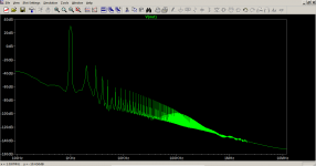
I am attaching the circuit, a Fourier distortion chart with a 2 Ohm load, and the output on short circuit (1 micro ohm).
The negative feeback network had to be forked into two sensing prongs with one at the output, and the other at the mid-potential of the VBE multiplier. To get such a midpoint two resistors, 47R, and two diodes, 1N4148, were added. A 33k resistor feeds the inverting input directly from the latter, so called, midpoint. Another, 39k, feeds the base from the output. Since, these two points are 'hypothetically' at the same varying voltage, calculation shows that to keep the previous amount of negative feedback, the 33k and 39k resistance must have a parallel value equal to 18k.
I have an uncomfortable feeling my changes, although they corrected the short circuit imbalance, are so unorthodox, that anyone who had been in electronics, may view them as problems, rather than a solution.
Needless to state, these changes have impacted the distortion figures negatively. The new distortion figures are:
a) 0.011% with 8R output
b) 0.042% with 4R output
c) 0.163% with 2R output
On hard short circuited output, 1 micro Ohm resistance, the quiescent currents are:
a) 15.95mA per output PNP transistor (2SA1943)
b) 10.51mA per output NPN transistor (2SC5200)
The output short circuit current is triangular with bases of around 26us and amplitude of 33A. The frequency is the simulated frequency of 1000Hz.
I am posting the circuit. I made a conscious effort not to change the original circuitry to enable myself to implement the new additions without having to rebuild the PCB from the very beginning.
I am attaching the circuit, a Fourier distortion chart with a 2 Ohm load, and the output on short circuit (1 micro ohm).
Attachments
Last edited:
Looking at the Fourier chart, one cannot fail to notice the third harmonic is quite strong although narrower than the second harmonic. Acoustically, the second harmonic may be acceptable as a distortion, but the third, many deem may sound unpleasant to the ear.
A drastic, but nevertheless easier way out of this, is to remove the short circuit protection altogether. The two pronged negative feedback network is sensing voltages where there is nothing of its business. The so called, midpoint potential of the VBE, should not be expected to move in synchrony with the output. At high current outputs this midpoint potential has to move above the output + 0.7V + some_extra_voltage. The latter extra voltage depends on the instantaneous current driven into the output.
A drastic, but nevertheless easier way out of this, is to remove the short circuit protection altogether. The two pronged negative feedback network is sensing voltages where there is nothing of its business. The so called, midpoint potential of the VBE, should not be expected to move in synchrony with the output. At high current outputs this midpoint potential has to move above the output + 0.7V + some_extra_voltage. The latter extra voltage depends on the instantaneous current driven into the output.
If you run the simulation I sent look at the visible traces for I (R21) and I (R24) which are very brief spikes which the output stage should be capable of handling. I did not adjust the standing current in this simulation so this is quite low and not equal for both halves so in that state it runs close to Class B the THD for sine wave input output of 50V peak. On a 8R load the peak current is 6A and when the output is dead shorted to ground this converts to a series of spikes up to 13A for 540uS between cycle swings I (L2). On 8R the 1kHz THD is about 0.02%.
The only high power CFP based power amplifier with short circuit protection that I have seen is one using Darlington power outputs which turns the output stage into a triple arrangement.
The protection circuit is far from simple and you don't want a major redesign after all the design effort you have put into this project.
When you consider the situation you have reached, 33A is a hazard to be reckoned with if it extends too long in terms of safe operating area for the combined output transistor set. I think it is likely to be a balancing act to reduce this without increasing THD which could be hard to swallow. In that case you would need to think whether rail fuses are a safer option and whether or not they compromise performance as much as the protection circuit does.
As I mentioned earlier your amplifier ought to be stable without that near short circuit for ac signals due to C10 - the 1uF capacitor loading the output. This will be spoiling your THD figures across the board
Earlier in this thread some posters mentioned the use of an input servo mechanism. This was mentioned as a measure to correct too high DC offsets. Although, the latest modifications do not suffer from overly high DC offsets, simulations are showing I can further minimize circuit modifications, by superposing a DC 64mV fed trough a 33k resistance to the non-inverting input. On hard output shortening the quiescent currents per output device is about 13mA. This solution does not negatively affect distortion and, more importantly, does not require the use of some exotic circuit modifications.
On a post earlier in this thread Mooly suggested an IC based input servo mechanism but I couldn't find it or a link to it. I remember it can easily get DC offsets down to nano volts.
The thing with the suggested servo is that it is a tried circuit unlike what I am doing. Sometimes, my thinking out of the box, makes think, I should have been in the arts, rather than technology.
- Home
- Amplifiers
- Solid State
- My attempts at a design of a 3 stage amplifier