Look at the first schematic with mosfet output stage post #1106
620 ohms to 33 ohms.
620 ohms to 33 ohms.
If you change one resistor to:
620 ohms to 33 ohms.
626 ohms to 33 ohms.
Amplitude is asymmetric.
THD rises.
I verified that in simulation
620 ohms to 33 ohms.
620 ohms to 33 ohms.
If you change one resistor to:
620 ohms to 33 ohms.
626 ohms to 33 ohms.
Amplitude is asymmetric.
THD rises.
I verified that in simulation
I think that you are ruining the high impedance of the Vas with a low end stage input impedance, thereby massively decreasing loop gain and thus distortion reduction.N and P mos have different saturation properties hence clipping is asymmetric (shows best at virtual earth, see pic)- no amount of feedback could correct that.
It will be most interesting to see the IM your amp produces at maximum output, with 1:1 11.5 KHz and 950 Hz.
Hans
The big cap in the second schematic seems to fix the symmetriy problem but now you have the big lytic there, maybe two big lytics back to back…
The ECW mos series used as source follower has a rather high input impedance, to the extent that a source follower doesn't result in THD / IMD improvement.I think that you are ruining the high impedance of the Vas with a low end stage input impedance, thereby massively decreasing loop gain and thus distortion reduction.
Hans
I see two BJT output transistors in your circuit diagram, so what do you mean with ECW mos series ?The ECW mos series used as source follower has a rather high input impedance, to the extent that a source follower doesn't result in THD / IMD improvement.

O.k.
Now to which circuit diagram does the mediocre IMD plot in #1113 belong, the one with BJT’s or with ECW’s ?
Rather confusing.
Hans
Now to which circuit diagram does the mediocre IMD plot in #1113 belong, the one with BJT’s or with ECW’s ?
Rather confusing.
Hans
To my understanding we have 3 topics here.
First schematic from Petr with mosfet output and 2 feedback path that can introduce errors.
Second schematic from Petr with BJT output from post 1113 where problem in nr.1 is fixed by a big cap and that has mediocre IMD.
3rd schematic from Aridace where he states that P and N devices are different which results in asymmetric clipping and feedback does not fix it.
Why? He loaded that bjt schematic in MC for his IMD test and found that it is rather poor but low order, so the amp could still sound ok.
Why then the reply with ECW’s on my comment that the Vas output impedance was ruined with the BJT’s low input impedance ?
With additional pre emitter followers result would have been much better.
With additional pre emitter followers result would have been much better.
I don´t know.Why then the reply with ECW’s on my comment that the Vas output impedance was ruined with the BJT’s low input impedance ?
With additional pre emitter followers result would have been much better.
Maybe he will clear that up.
Small update:
I made a simplified line level buffer from my schematic, THD is -225 dB, for the full version I expect -250 dB or better.
Problem: MC12 transient analysis seems to be limited to -260 dB. Any chance to improve that with settings ?
Black is the sine source, red my amplifier.
Last edited:
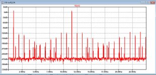
With just a bit fiddling and increasing the loop gain, I could lower IMD by 30dB still without any optimization.
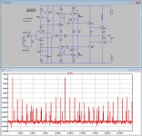
Left the original and a the right the modified version, both having 850mA bias current.
Hans
Left the original and a the right the modified version, both having 850mA bias current.
Hans
Attachments
Last edited:
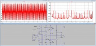
And when removing the 1m cap over the two 33R resistors, IMD spectrum becomes even better.
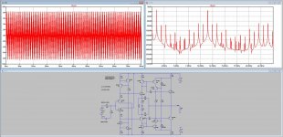
Schematic from post 1112 and 1113
THD with cap is worse than without.
Same for THD 😊
Without the cap, try IMD with one of the 330 ohms feedback resistors changed to 333.3 ohms (+1%)
So many amps are being discussed that confusion about "which amp?" is likely. I only simmed IMD (950,11500 1:1) for that Hiraga amp with bjt.I see two BJT output transistors in your circuit diagram, so what do you mean with ECW mos series ?
In my amps I would only use bjt as EF, when driven by low distortion opamp.
Well, that's the easiest problem to solve, just replace the four 330R and 33R resistors by one 160R and one 16R resistor.Same for THD 😊
Without the cap, try IMD with one of the 330 ohms feedback resistors changed to 333.3 ohms (+1%)
The four 10R emitter resistors are just there to linearize non ideal diamond transistors, but don't affect gain.
With this mod, resistor matching is no longer an issue.
It simply shows that this Hiraga design is not well developed to its ultimate potential.
There is probably even more to improve, but a few steps already improved IMD by 44dB to below -125dB, not that bad at all.
Hans
Attachments
- Home
- Amplifiers
- Solid State
- Musings on amp design... a thread split