The DAC will need two power supply voltages.
One 5V and one 3.3V. I am working on a PCB for that too. But just about any power supply at those voltages will be fine.
One 5V and one 3.3V. I am working on a PCB for that too. But just about any power supply at those voltages will be fine.
Your silkscreen notations for the jumper settings will end up as indecipherable blobs, they are way too small and too fine.
Does that qualify me as a beta tester? 🙂
Does that qualify me as a beta tester? 🙂
pinkmouse said:Your silkscreen notations for the jumper settings will end up as indecipherable blobs, they are way too small and too fine.
Does that qualify me as a beta tester? 🙂
Good point. 🙂
The PCB Fab says they are within spec, but we will leave the documentation for jumper settings here and on our site so if people get blobs we won't be out of luck. 🙂
If you want in on the test then your in.
Cheers!
Russ
Ta!
I'm actually supposed to be working at the moment, so I didn't have more than a quick glance. I'll have a better look when I get home. 😀
I'm actually supposed to be working at the moment, so I didn't have more than a quick glance. I'll have a better look when I get home. 😀
I'm actually supposed to be working at the moment
Well, that's no excuse... so are we!! 😉
Shhhh!
It's ok, I just printed everything out on the works printer for later perusal! 😉
Oh, and anther quick point, can you move the component designators out from under the footprints? It makes fault finding so much easier. Not a great problem with the number of components on this board, but a good habit to get into.
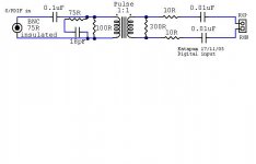
I know I am late 😉 The input stage could use some refinement IMHO. I would load the primary side after the cap with 150 Ohm and I would load the secondary side with 150 Ohm too. Definitely keep the input cap, it protects the pulse transformer from DC. A 10 kOhm from the SPDIF-2 to GND wouldn't hurt, it will keep the primary side at low potential when switching cables with the DAC powered on. I used this circuit a lot ( also for inspiration ) but please note that it uses a 1:4 transformer:
http://members.brabant.chello.nl/~m.heijligers/DAChtml/dig_r2a.pdf
*It is adviseable to use a 75 Ohm BNC chassis connector directly on the PCB for optimal results as standard PCB connectors really aren't suitable 75 Ohm devices. Please see the DAC Peter Daniel designed to see what I mean. The circuit with SN75179 also works well but IMO the guideline with semiconductors is that "less is more"....
When I was searching for the right thread I stumbled upon this one that I did not try ( to me both the caps and the 10 Ohm resistors at the secondary side seem useless but I may be wrong ) but you'll get the idea:
Attachments
BTW did I mention I'd like to be beta tester as well ? If you appreciate further comment please let me know. I have some other suggestions.
jean-paul said:BTW did I mention I'd like to be beta tester as well ? If you appreciate further comment please let me know. I have some other suggestions.
Your in,
Let, me see what I can do about your suggestions.
Keep in mind I did not anticipate the PCB being directly mounted to a chassis, so I have not provided for PCB mounted BNC or RCA. Instead I was going to allow for chassis mounted connectors which would be wired to the PCB via the terminals. This may not be optimal, but it is very practical...
Cheers!
Russ
Am I right in thinking you are using a power plane and a ground plane? Would you not be better off with a ground plane both sides with loads of vias, and power tracks?
pinkmouse said:Am I right in thinking you are using a power plane and a ground plane? Would you not be better off with a ground plane both sides with loads of vias, and power tracks?
The datasheet encouraged the use of both a power and GND plane.
BTW I am reworking the silkscreen(had some flubbage) and layout a bit based on the input so far.
Jean Paul,
I think I can work it so that we have a PCB mounted BNC, those who do not want to mount the PCB to the chassis can simply wire to the pads, or I may have alternate pads for the terminal block.
I will post the changes tomorrow.
Jean Paul,
I think I can work it so that we have a PCB mounted BNC, those who do not want to mount the PCB to the chassis can simply wire to the pads, or I may have alternate pads for the terminal block.
I will post the changes tomorrow.
Fair enough. I suspect that's one for those lucky enough to have lots of high tech measuring equipment to decide.
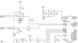
Optical would certainly allow a little more flexibility, maybe it could be added as a separate routed section, (perhaps attached to the PSU board), that could be piggy backed onto the main board for those that want it.
With this particular DAC all we need is a small capacitor and a pair of solder pads. Pretty cheap in terms of effort and PC board real estate to gain a lot of flexibility.
-David
-David
- Home
- More Vendors...
- Twisted Pear
- Mr White's "Opus", designing a simple balanced DAC