Can't you just use it in an LTP input stage biased by a CCS ?
Then the current (and hence dissipation) is determined by the CCS, independent on Idss.
For example Mr. Evil's :
All JFET open-loop RIAA pre-amp
Patrick
Then the current (and hence dissipation) is determined by the CCS, independent on Idss.
For example Mr. Evil's :
All JFET open-loop RIAA pre-amp
Patrick
It should work like this:
Could not raise current higher than 21mA per jfet otherwise drain load becomes too small
As it is now, gain in 1st stage is 48dB for a total gain of 62dB
R16 is the cart loading resistor (1k)
Coupling caps can be green bipolars 10u
R7 (now 400) sets second stage gain
Q1 should be heatsinked
NFB shunt resistors set to 3.9ohm
IF3602 model came from interfet list and can be ameliorated if you have data from a real device.
Attachments
Unfortunately I could not make it work with the base grounded..... In that case the current setting resistor (R13) becomes very small and LTSpice did not give a good solution.
I would like to use a bigger value fro R13 (as that way CCS output impedance would be higher) but two leds are a good compromise.
Please bear in mind that we are running this CCS at near 40mA
I would like to use a bigger value fro R13 (as that way CCS output impedance would be higher) but two leds are a good compromise.
Please bear in mind that we are running this CCS at near 40mA
Last edited:
This is not in agreement with schematic in post 11385,
the emitter resistor must be larger than with your small
reference voltage.
The r. v. in the original set up is the negative supply.
the emitter resistor must be larger than with your small
reference voltage.
The r. v. in the original set up is the negative supply.
If most of the emitter current is going through R6
and R9 purpose of the current source is defeated ..
and R9 purpose of the current source is defeated ..
I had a look at the circuit in #11410, and have a number of comments:
1) C15/C16 have no function, they can be omitted saving quite some PCB space.
2) The junction between C2/C3 and C13/C1 are connected to Gnd, this has no function.
3) Output amp U8 has 3k3 and 10K resistors, more logical would be all four 3k3 or all 10k.
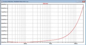
When measuring the equivalent input noise with a 0R source resistance, I get 0.71nV/rtHz A-Weighted which is good but not excellent for this very expensive dual Fet.
With a 10R source EIN becomes 0.73nV/rtHz A-weighted.
See calculated input noise below with 10R source.
Hans
.
1) C15/C16 have no function, they can be omitted saving quite some PCB space.
2) The junction between C2/C3 and C13/C1 are connected to Gnd, this has no function.
3) Output amp U8 has 3k3 and 10K resistors, more logical would be all four 3k3 or all 10k.
When measuring the equivalent input noise with a 0R source resistance, I get 0.71nV/rtHz A-Weighted which is good but not excellent for this very expensive dual Fet.
With a 10R source EIN becomes 0.73nV/rtHz A-weighted.
See calculated input noise below with 10R source.
Hans
.
Attachments
I had a look at the circuit in #11410, and have a number of comments:
1) C15/C16 have no function, they can be omitted saving quite some PCB space.
2) The junction between C2/C3 and C13/C1 are connected to Gnd, this has no function.
3) Output amp U8 has 3k3 and 10K resistors, more logical would be all four 3k3 or all 10k.
When measuring the equivalent input noise with a 0R source resistance, I get 0.71nV/rtHz A-Weighted which is good but not excellent for this very expensive dual Fet.
With a 10R source EIN becomes 0.73nV/rtHz A-weighted.
See calculated input noise below with 10R source.
Hans
.
There is no compensation C in opamps local feedback path typical for this
type of circuit. Omitting this with IF3602 is asking for trouble.
WRT noise -> 3 x 2sk369 or equiv / phase will get very similar results.
Has anyone done a distortion sim at say 60dB gain?
TCD
If you parallel the two FETs in a LSK389 you can get 0.63nV based on a typical en figure of 0.9nV per JFET. See X-Altra link below for full details.
Of course the IF3602 has other great features that the LSK does not.
🙂
Of course the IF3602 has other great features that the LSK does not.
🙂
…
3) Output amp U8 has 3k3 and 10K resistors, more logical would be all four 3k3 or all 10k
...
.
Not so, see my answer/remark/comment (before/earlier) to RCruze.
Last edited:
Frans, I can't find your answer to RCruz. But from my own measurements, it makes sense to make the two pairs different rather than equal value.
The input impedance of the two legs is quite different, and if you want to load the diff amp equally on both outputs (a requirement for balanced lines!), you need to have the two pairs different.
IIRC the ratio should be 1:4 (or was it 1:3? Can't remember).
Jan
The input impedance of the two legs is quite different, and if you want to load the diff amp equally on both outputs (a requirement for balanced lines!), you need to have the two pairs different.
IIRC the ratio should be 1:4 (or was it 1:3? Can't remember).
Jan