We wrote about schottkies don't need di/dt limit during turn-off. So the efficiecy can be improved because the dissipation under the transition is a similar amount of the dissipation under the conduction of MOSFETs.
Can you post a schematic about those SS circuits?
Can you post a schematic about those SS circuits?
Hmmm... 🙁 That IGBT amplifier could be very promising. I am planning to make an amplifier in a few tens of kW range. But my scematics also haven't been made. Maybe the UcD is the best choice because of his analog sigma-delta like theory.
Just jokin buddy,
we manufacture professional amps with Class-AB, Class-D topologies
Pro-audio gear
we manufacture professional amps with Class-AB, Class-D topologies
Pro-audio gear
Yeah IGBT was choosen for higher power, but was discontinued because we have achieved our targetted objective of 5KW with Class-D topology in a much efficient manner...
Could you reduce the dead-time caused flattening in the class-d output linearity function too? Has it an effect in the audio fidelity?
Last time I thought about unite the UcD with a repose duty factor controlled BCA in theory. But I haven't pass it out. For example, his name could be UcDBCA  Is there anybody who regards it as a good idea?
Gyula
Is there anybody who regards it as a good idea?Gyula
Hi Gyula,
you would have to sacrifice main point of BCA technology, that is ripple cancelation, since UcD depends on output capacitor ripple voltage for oscillation. But I think it might be feasible.
Best regards,
Jaka Racman
you would have to sacrifice main point of BCA technology, that is ripple cancelation, since UcD depends on output capacitor ripple voltage for oscillation. But I think it might be feasible.
Best regards,
Jaka Racman
I got a great deal of efficiency improvement and EMI reduction when I added a 45A/us magnetic snubber to my continuous mode 2KW boost PFC converter. As in class D amps, it's required to switch over a conducting diode on each cycle, and it's not a nice 200V or 100V diode, but an inherently slow 600V one (a couple of MUR860) whose negative current recovery spike becomes huge if a too high di/dt is employed. Also, note that the voltage switched is not the harmless 100V seen in class D amplifiers but 440V, that can make the IGBTs and the diodes explode due to enormous reverse recovery currents if you try to switch too hard without any di/dt control.
The following picture shows a basic schematic:
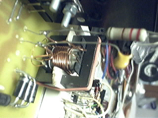
L2 and L3 constitute a coupled inductor wound on the same gapped ferrite core with a 3:1 turns ratio and 30A saturation to accomodate load and diode reverse recovery currents. The lower side of L3 will rise 1.760V above ground during diode recovery as 440V (output) are being applied to L2 and the inductor is energized, then it will return the excess energy to ground through these four 600V 4A diodes and the rest will be returned at turn-off. After all the energy has been returned, the system is ready for another switching event, thus imposing a minimum off period of three times Trr. The 3:1 turns ratio is chosen to produce 586V on the upper leg of L2 during discharge, just below the Vce limit of the IGBTs (actually some avalanche happens during some 25ns at full load due to leakage inductance, but that's harmless in comparison with what happens when you switch directly over the diode).
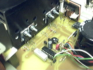
These two pictures show the working magnetic snubber and the 2KW PCF prototype. Note how 2KW at 440V DC output are obtained at 160V AC input with just four ridiculous TO-220 devices (they would explode without the snubber, yet they produce considerable output before requiring a fan with it). Note also the "relaxed" layout, only possible thanks to the limited di/dt switching.
Currently I'm developing a class-D-like mains sine inverter with the same IGBTs, the same high voltages, and the same diode recovery problems in it, so I don't discard applying these techniques to boost efficiency (and reliability) if required. That could be best achieved by employing two primaries in the coupled inductor, one in series with each collector, with additional diodes and some control tweaks to force a minimum off-time.
The following picture shows a basic schematic:
An externally hosted image should be here but it was not working when we last tested it.
L2 and L3 constitute a coupled inductor wound on the same gapped ferrite core with a 3:1 turns ratio and 30A saturation to accomodate load and diode reverse recovery currents. The lower side of L3 will rise 1.760V above ground during diode recovery as 440V (output) are being applied to L2 and the inductor is energized, then it will return the excess energy to ground through these four 600V 4A diodes and the rest will be returned at turn-off. After all the energy has been returned, the system is ready for another switching event, thus imposing a minimum off period of three times Trr. The 3:1 turns ratio is chosen to produce 586V on the upper leg of L2 during discharge, just below the Vce limit of the IGBTs (actually some avalanche happens during some 25ns at full load due to leakage inductance, but that's harmless in comparison with what happens when you switch directly over the diode).
These two pictures show the working magnetic snubber and the 2KW PCF prototype. Note how 2KW at 440V DC output are obtained at 160V AC input with just four ridiculous TO-220 devices (they would explode without the snubber, yet they produce considerable output before requiring a fan with it). Note also the "relaxed" layout, only possible thanks to the limited di/dt switching.
Currently I'm developing a class-D-like mains sine inverter with the same IGBTs, the same high voltages, and the same diode recovery problems in it, so I don't discard applying these techniques to boost efficiency (and reliability) if required. That could be best achieved by employing two primaries in the coupled inductor, one in series with each collector, with additional diodes and some control tweaks to force a minimum off-time.
Hmm, interesting. The TI UCC3855 does the soft switching with two transistors. The things would be more simple if SiC diodes could be used. I have seen 30A 600V SiC diodes at APT two years ago. And then this type of semiconductor was disappeared from their site. I don't know why.. 🙁 The SiC diodes are also have metal-semiconductor junction. So they could be switced as fast as you don't spare the trouble, with respect of their capacitance.
Jaka, you are right. This is a serious difference. 😀
Jaka, you are right. This is a serious difference. 😀
SiC diodes are not a real solution, they have been around for several years now (probably a decade), yet they seem to have a lot of trouble entering the market and becoming industry standard. These diodes are said to feature nearly zero recovery time and little or no recovery current, but what they don't say is that the nominal voltage drop at rated current is between 3V and 5V, so you end up trading some switching losses and EMI for more conduction losses (forget about paralleling them with MOSFET body diode). That pitfall together with their insane price makes them not such a good alternative (I'm not going to pay $50 for each damn 30A diode).
Concerning the scheme employed with the UC3855 to prevent hard switching over the diode, it's quite complex and requires not only an additional inductor but also more diodes, swithces and active control. I considered it at the beginning, but I opted for the magnetic snubber since it forces not only diode recovery but all the transitions to happen at a fixed current rate (this makes a whole difference in EMI terms). Also, I found out empirically that the continuous mode PFC converter inherently satisfies the minimum-off-time condition, as duty cycle is inversely proportional to voltage and current, so the shortest off-times happen when snubber discharge times are also very small, thus never leading to hard switching.
Concerning the scheme employed with the UC3855 to prevent hard switching over the diode, it's quite complex and requires not only an additional inductor but also more diodes, swithces and active control. I considered it at the beginning, but I opted for the magnetic snubber since it forces not only diode recovery but all the transitions to happen at a fixed current rate (this makes a whole difference in EMI terms). Also, I found out empirically that the continuous mode PFC converter inherently satisfies the minimum-off-time condition, as duty cycle is inversely proportional to voltage and current, so the shortest off-times happen when snubber discharge times are also very small, thus never leading to hard switching.
Jaka Racman said:Hi Gyula,
you would have to sacrifice main point of BCA technology, that is ripple cancelation, since UcD depends on output capacitor ripple voltage for oscillation. But I think it might be feasible.
Best regards,
Jaka Racman
Gyula said:Hmm, interesting. The TI UCC3855 does the soft switching with two transistors. The things would be more simple if SiC diodes could be used. I have seen 30A 600V SiC diodes at APT two years ago. And then this type of semiconductor was disappeared from their site. I don't know why.. 🙁 The SiC diodes are also have metal-semiconductor junction. So they could be switced as fast as you don't spare the trouble, with respect of their capacitance.
Jaka, you are right. This is a serious difference. 😀
Is it time for an open source ultimate class d project yet?
BTW at this time I'd like to share this finding for discussion:
http://www.freepatentsonline.com/5332938.pdf
I see that patent mostly useless (at least without a lot of additional complexity). When switching over a diode, a negative spike will come to the drain after the positive spike because recovery current is substantially higher than load current, but that inductor won't have any other discharge path than the gate  In fact, source parasitistic series inductance spikes are one of the reasons why MOSFETs blow unexpectedly in DIY SMPS prototypes when the builder is not aware of layout requirements.
Why they don't patent useful things? 😀
In fact, source parasitistic series inductance spikes are one of the reasons why MOSFETs blow unexpectedly in DIY SMPS prototypes when the builder is not aware of layout requirements.Why they don't patent useful things? 😀
That patent isn't telling of the whole circuit used though, I'd imagine another compensation network used from drain-gate?
If you try to fix it so that it can work, you end up with something very similar to my circuit but connected in the source/emitter side 😀 It's far more convenient to place the inductor in the drain/collector, though, and leave it see all the supply voltage during turn-on.
Eva said:If you try to fix it so that it can work, you end up with something very similar to my circuit but connected in the source/emitter side 😀 It's far more convenient to place the inductor in the drain/collector, though, and leave it see all the supply voltage during turn-on.
😎
That's about what I was thinking too.
Someone on sci.electronic.design really tried to rip that patent apart a few years back and eventually discovered the extra work required to make it happen.
I think I can easily agree with what you're saying.. and btw, nice to see you in the class d section.
- Status
- Not open for further replies.
- Home
- Amplifiers
- Class D
- Mosfet driver IC's