Since all of ADIs LDOs are in smd packages only chip caps are considered practical. Only the ESR is spec'ed since the ESL of the ceramic caps very small and not an issue for the feedback loop. The loop is stable with ESRs as low as 100 micro-ohms which is why there isn't a lower limit, the interconnect resistance will be greater than that.
The ADM715x were never intended for fast transient response since VCOs and PLLs present fairly static loads.
I am a little confused as to why the ADM7150 worked poorly with a DAC. Can you tell me what the part number is?
The ADM715x were never intended for fast transient response since VCOs and PLLs present fairly static loads.
I am a little confused as to why the ADM7150 worked poorly with a DAC. Can you tell me what the part number is?
Last edited:
I actually use 2 of these, one 3.3V for driving the 24.576MHz crystal oscillator and its buffer - which is the intended purpose of this regulator, I gather. The other is a 5V for WM8741 DAC where it should be an overkill, I wanted to use ADP150 initially. I followed the layout recommendations from the datasheet except for output cap. I've seen regulators - usually Jung style or other discrete ones - oscillate but this "working just not well" behaviour is new to me. I'm not a professional though, just a hobbyist.
Is polymer cap still ok to be used for bypass pin capacitance (in parallel with a smaller ceramic)? That's also what I'm using it for.
In next iteration I will definitely go to using a 0805 ceramic in a same position as in datasheet layout and maybe add an optional cap on the side to play with.
Is polymer cap still ok to be used for bypass pin capacitance (in parallel with a smaller ceramic)? That's also what I'm using it for.
In next iteration I will definitely go to using a 0805 ceramic in a same position as in datasheet layout and maybe add an optional cap on the side to play with.
It's the largest cap with the lowest ESR available in that voltage.
Why do you want "lowest ESR available" ? What you need is "the right amount of ESR".
The last time I used a really low ESR polymer cap like this, was because I needed a very small cap that could take the ripple current out of a DC-DC without exploding.
normally less ESR is a good thing.
If you put several amps of ripple current in a cap half the size of a fingernail, then yeah.
Otherwise, no. The Good Thing is Damping factor of your PDN >1.
I did not have a ceramic cap in parallel at all though, just a small SMD film cap but a few cm away so I was not counting it.
SMD ceramic and film have about same ESL/ESR for the same package size.
If it is a bit far like you say, this means more inductance. Remember damping factor is R/2 sqrt(C/L) ; more L means more trouble, less C also means more trouble. 100nF capacitors pretty much guarantee failure (unless you got 100 of them).
I am just surprised that any of this would make that much difference at only a few MHz.
Resonance between polymer cap and next smaller cap is usually around this frequency...
>> Otherwise, no. The Good Thing is Damping factor of your PDN >1.
Do you mean damping of signal injected into power rail by the device being powered?
>>SMD ceramic and film have about same ESL/ESR for the same package size.
Of course.
>If it is a bit far like you say, this means more inductance. Remember >damping factor is R/2 sqrt(C/L) ; more L means more trouble, less C also >means more trouble. 100nF capacitors pretty much guarantee failure
>(unless you got 100 of them).
But if it is sufficiently far then the resistance of the trace would effectively neutralize that, no? Oscillator won't do much oscillation if there is a too much resistance in the loop. Which is why I didn't count it.
>Resonance between polymer cap and next smaller cap is usually around >this frequency...[/QUOTE]
Yes and that is what we all rely on, paralleling caps with different resonant frequencies to try to get a "flat" response in a wider frequency range than with just one cap. What I meant is that I did not expect that ESL of the polymer or the interaction with the PCB to affect that well know diagram with two dips, where you have the "big" cap bottom out at a MHz or two and then next cap at 10MHz and so on. Your description sounded like that a different situation would happen when using low ESR SMD polymer. I was just surprised as I usually hear people start talking about trace impedances, board parasitics and such, when we get to much higher frequencies.
As for ESR, since this is still a regulator, there is some power supply ripple and low ESR reduces ripple, so I usually go for lower ESR in order to get rid of 60Hz and its harmonics as much as possible. As long as it doesn't make anything unstable of course.
Last edited:
After hacking a 10uF 1206 ceramic, I see you are right that the slightly remote film cap is a problem. It is only a 10nF cap but if it remains in parallel with a ceramic, the results are still bad. Significantly better than with polymer but I needed to remove the film cap to get another dramatic improvement. I am judging just on harmonics showing up on DAC output, and I see 10dB improvement with each of those steps which is huge. Interestingly, just an older small Os-Con in a can, in parallel with that film cap, gives about the same results as just a ceramic by itself. Looks like I have a lot of work to do with the layout and cap selection. Thanks for tips.
Rule Number one for laying out these types of supplies (and any other)...
Cin, Device and Cout 0V (GND, GROUND) connection needs to be one points, or as near as dammit, with the lowest possible inductance etc., all on the same side of the board...
Follow this simple rule and you are on your way to optimising the PSU for the lowest possible noise.
What you are doing is minimising the input/output loops that often have noise, ripple etc. (these are generally referred to as AC or switching loops) and this is critical to getting the best out of any power supply.
Rule 2, feedback inputs are critical 🙂
Do you mean damping of signal injected into power rail by the device being powered?
I mean damping factor of series RLC circuit is zeta = R/2 sqrt(C/L)
When you parallel two caps, you get a series RLC with R and L as the sum of both caps and traces ESRs and ESLs, and C is the two caps in series.
If zeta is too low you get ringing, ugly transient response, and an impedance peak.
Since your caps are part of the LDO feedback loop, the impedance peak gives extra gain in the open loop response, at a frequency where the LDO perhaps does not have that much phase margin. The peak also produces a 180° phase rotation. This can have lots of funky effects on the transient response.
But if it is sufficiently far then the resistance of the trace would effectively neutralize that, no?
Further = more R but also more inductance, so it depends.
What I meant is that I did not expect that ESL of the polymer or the interaction with the PCB to affect that well know diagram with two dips
Well pretty much everything in this "two dip diagram" is dependent on parasitics, so they can move around a lot... and the PCB is the MAJOR hidden component.
Your description sounded like that a different situation would happen when using low ESR SMD polymer.
Well the difference is that it has lower ESR, so it has lower damping, so it needs more attention.
Can you describe the schematic (with cap types and values) and layout that made this regulator misbehave ? Did you by any chance have a 100nF cap somewhere ?
As for ESR, since this is still a regulator, there is some power supply ripple and low ESR reduces ripple, so I usually go for lower ESR in order to get rid of 60Hz and its harmonics as much as possible.
If you want a ripple filter then put the polymer cap on the input and add a 0.033R resistor between it and the 10uF MLCC at the input of the reg.
Rule Number one for laying out these types of supplies (and any other)...
Cin, Device and Cout 0V (GND, GROUND) connection needs to be one points, or as near as dammit, with the lowest possible inductance etc., all on the same side of the board...
Follow this simple rule and you are on your way to optimising the PSU for the lowest possible noise.
What you are doing is minimising the input/output loops that often have noise, ripple etc. (these are generally referred to as AC or switching loops) and this is critical to getting the best out of any power supply.
Rule 2, feedback inputs are critical 🙂
I normally try to copy the layout what they use on their evaluation boards. Especially for feedback and NR pins where as you say it is critical to prevent noise injection. But for output and input caps I usually make changes. In this case it didn't work out 🙁 .
>I mean damping factor of series RLC circuit is zeta = R/2 sqrt(C/L)
I am familiar with this (I won't say I would be able to solve the differential equation) but just for clarity sake, who is damping what? I presume we are modelling only the output of the regulator with the connected capacitor loops, and then looking at how will voltage look like when we have device under power drawing non-constant current? So we are looking at how bypass caps (and all their parasitics) are behaving when some transients are injected?
>When you parallel two caps, you get a series RLC with R and L as the sum of both caps and traces ESRs and ESLs, and C is the two caps in series.
Normally the formula for two parallel impedances that have both C and L components gets really ugly, but since the parasitic impedance (L) is small compared to what the component is (C), does it end up approximated by the one you wrote? C being two caps in series is counter intuitive.
>If zeta is too low you get ringing, ugly transient response, and an >impedance peak.
Yes.
>Since your caps are part of the LDO feedback loop, the impedance peak >gives extra gain in the open loop response, at a frequency where the LDO >perhaps does not have that much phase margin. The peak also produces a >180° phase rotation. This can have lots of funky effects on the transient >response.
Yes, that certainly makes sense. I guess this is why almost all regulators heavily compensate so no matter what you connect, it remains stable but at the cost of very low bandwidth where you actually get regulation. I recall similar situation for Jung regulator where using it to power a circuit with the usual big bypass caps just make the whole thing oscillate.
Does this mean that the use case for this regulator is strictly powering a very close by component or two, with no additional bypass caps on those components? I can't see this being used to drive a power "rail" with a bunch of components at various lengths away, each with its own bypass cap or two. If the use case is powering up a crystal oscillator, PLL chip or the like, I imagine that is the only thing you'd have tied to the regulator anyway. In my case that is exactly how I used it - one regulator only for DAC chip, and the other one to drive XO and the Potato buffer, and I used a more typical regulator for digital supplies of other chips anyway.
>Further = more R but also more inductance, so it depends.
You were right, it looks like the added R was too little to make a big dent in damping factor.
>Well pretty much everything in this "two dip diagram" is dependent on >parasitics, so they can move around a lot... and the PCB is the MAJOR >hidden component.
I just didn't expect PCB to play a major factor at only a few MHz. From my previous readings of various app notes, conference PDFs and the like, I would not have expected that until closer to 100MHz. Though in this case you reckon it is the inductance that makes a difference, not capacitance.
>Can you describe the schematic (with cap types and values) and layout that >made this regulator misbehave ? Did you by any chance have a 100nF cap >somewhere ?
It was just a 200uF 6.3V 9mOhm polymer cap (SMD but these are large) right at the chip but on the opposite side (so vias are used) - don't ask me why I didn't put at least a small ceramic right on top, it was stupid of me - and a 0805 10nF PPS film cap. about 1-2cm away, also on the opposite side, right under the dac chip (with all 3 of its power supply pins converging at that point). Yesterday, I put the 10uF 25V X7R 1210 cap on top very close to chip (between via point and the scrached off ground plane/copper pour) which improved situation (2nd harmonic of DAC was 10dB better) but still well below what it should be. Then I removed the 10nF film cap and it improved another 10dB. I then added another 10uF X7R 0805 where the film cap used to be and later also an older 47uF 6.3V OS-CON canned cap (+10 years old so not the lowest of ESR though probably still quite low) where the big SMD polymer used to be and each of those gave me a few more dB improvements. Results are now within what I would expect but obviously I have no idea if everything is at 100% or 90%, as DAC produces 0.0025% distortion and harmonics are still a bit higher than what they should be. I am OK with using just one or two 10uF ceramics but it doesn't seem to be quite enough. I am not sure what equipment I need to in order to investigate this.
>If you want a ripple filter then put the polymer cap on the input and add a >0.033R resistor between it and the 10uF MLCC at the input of the reg.
Another excellent suggestion, thank you.
Normally the formula for two parallel impedances that have both C and L components gets really ugly, but since the parasitic impedance (L) is small compared to what the component is (C), does it end up approximated by the one you wrote? C being two caps in series is counter intuitive.
Yes it is a series RLC.
A simple model of a capacitor is R, L, C in series.
C is the capacitor.
L is the capacitor ESL, plus the mounting ESL. For example a 6.3mm diameter capacitor with 2.5mm pin spacing will have about 3.5 to 4 nH. Mounting inductance is the inductance of a square loop of (pin spacing x pcb height), in your case about 1 nH. It will be reduced for mutilayer PCBs if the GND/power planes are the side close to the cap. If the cap is mounted crooked and/or not touching the PCB then ESL also increases, of course.
R is the capacitor ESR plus the mounting ESR which is usually negligible.
So you got your capacitor. It's a simple model without dielectric absorption, skin effect or RF effects but it's pretty good for our purposes.
Now if you put two capacitors in parallel (draw the two RLC models on a paper and connect them together), you'll notice you get a RLCRLC series circuit, that you can simplify by grouping together the elements of each kind.
So, you get a series RLC with :
R = both ESR in series
L = both ESL and mounting L in series
C = both caps in series (this is what got you, since 200 µF in series with 10nF is still about 10nF)
So to study the resonance of two caps in parallel, you need to apply the series RLC formula 😀
just for clarity sake, who is damping what?
I was only talking about the seemingly simple case of two caps in parallel...
Does this mean that the use case for this regulator is strictly powering a very close by component or two, with no additional bypass caps on those components? I can't see this being used to drive a power "rail" with a bunch of components at various lengths away, each with its own bypass cap or two.
If you use a low noise regulator, you're probably going to dedicate it to a specific load. It would make no sense to share it with a noisy load like a cpu. If several loads use the same regulator, then they'd all have to be "civilized" (ie, drawing mostly constant current), because just a few mA variable current in 1 mOhm impedance, and you no longer have a 1µV noise regulator...
Also if you put several loads and the last one is a bit far away, and you got more than a few µV noise in the GND between its location and the regulator, then again you no longer have a 1µV noise regulator...
But I don't see why it wouldn't be able to power several loads... as long as the PDN for them is actually designed (not random)
> I just didn't expect PCB to play a major factor at only a few MHz.
When you got a cap with too low ESR, then you need low inductance, and the moment you start counting nH and measuring loop areas, you're kinda doing HF design, even if it's at low frequencies. Same for switching converters...
> It was just a 200uF 6.3V 9mOhm polymer cap
> and a 0805 10nF PPS film cap. about 1-2cm away
Ah, ok. If you put a 10nF decoupling cap then failure is not just an option, it is pretty much inevitable 😀
If you calculate the damping factor of a 10nF cap in parallel with your low ESR cap you will notice it is something like 0.01 ; in other words a nice tuned resonator with a huge peak and pretty high Q.
> Then I removed the 10nF film cap and it improved another 10dB.
Yeah 😀
> I am OK with using just one or two 10uF ceramics but it doesn't seem to be quite enough.
Looking at the output impedance of the reg posted earlier, 1 or 2 10µF caps seem ideal 😉
That's what the designer of the regulator intended, he put his poles at the right spot for this scenario.
Now if you put two capacitors in parallel (draw the two RLC models on a paper and connect them together), you'll notice you get a RLCRLC series circuit, that you can simplify by grouping together the elements of each kind.
Oh you are talking about a loop that includes JUST the two caps in parallel? Yeah in that case it will be exactly as you say of course. I thought you are talking about a loop from the device under test - or regulator - that goes through an abstract RLC circuit that is our two caps in parallel. In that case you have the ugly formula I linked to at earlier.
You're right, I wasn't thinking. I recall reading a paper about effects of all those paralleled bypass caps all over the place and loops between them. I have been using ferrite beads between power rails and each chip's VCC pin for over 10 years now. This would have the effect of adding a large-ish resistance at MHz range and preventing any of the loops from having low damping factor. But it does nothing if caps are in parallel, however this is usually what we want (keep the impedance low in wide range).
When you got a cap with too low ESR, then you need low inductance, and the moment you start counting nH and measuring loop areas, you're kinda doing HF design, even if it's at low frequencies. Same for switching converters...
Yikes, I have no $$$ software or the black magic experience to be doing that. I thought I am staying safe playing at a few MHz (ignoring clocks).
Ah, ok. If you put a 10nF decoupling cap then failure is not just an option, it is pretty much inevitable 😀
I'm lucky that most components are tolerant of crappy engineering. This chip on the other hand does not tolerate incompetence. It's interesting because even with this problem it would still probably seem good enough and I'd never find out about this, except that WM8741 seem to have no PSSR *at all* on its own, at least in lower audio band. If I was powering up a normal opamp which has no such problems, it would have likely looked fine. On the other hand this seems to justify using an expensive high PSRR wide bandwidth low noise regulator for it - as long as you use it correctly.
Looking at the output impedance of the reg posted earlier, 1 or 2 10µF caps >seem ideal 😉
That's what the designer of the regulator intended, he put his poles at the right spot for this scenario
What I meant is that even with two capacitors I was not getting best results. It looked good enough but not great. Adding the oscon as an experiment improved results noticeably though not hugely. That leads me to believe my particular board layout needs to be revised to match evaluation board as right now it doesn't interact with those capacitors in the way regulator designed expects. Either that or I need to experiment until I find a satisfactory solution. From all you said that is not surprising at all.
So this means that any design with this chip pretty much has to ensure that the poles caused by cap(s) go exactly where the designer of the chip expected them to, at least those that fall within range where gain is >1?
This reminds me of a SPICE sim we did at university as a project / contest to see who can design an amplifier with least transistors and given bandwidth. It deteriorated into throwing inductors in and then trying to flatten the frequency response. We were trying to null the poles and every time you tweak one capacitor or inductor it would have a domino effect. I recall it was finicky as hell. And that was just a sim.
Can those "two peak" graphs be drawn using a function generator (say sweep from 100kHz to 10MHz) and an oscilloscope? I mean measured on the PCB without regulator and the load. I would really like to be able to see the effects of changes on screen or paper somehow.
The last 2 pages are making this too complex - this is not a difficult regulator to use. It's performance is excellent even with through-hole components.
The last 2 pages are making this too complex - this is not a difficult regulator to use. It's performance is excellent even with through-hole components.
I agree 😀
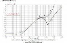
Actually if you look at the output impedance curve of this regulator, you'll probably notice the thing is pretty clever.
It has very low DC impedance, but the transition to 10uF MLCC is smooth and the transient response is near perfect. In fact it has the optimum impedance curve for a regulator using only a 10u MLCC on the output. It is impossible to do better unless you add a real crapload of capacitors, or you replace the MLCC with something else.
This is also impossible to do with a simple open loop function having a single pole, like an Opamp Superreg. These can never be rock-solid with a MLCC on the output unless the compensation is tweaked.
I'd bet that the ADM7150 output Z (without the capacitor) looks like this crappily hand-drawn curve.
Pole @ 2kHz
Zero @ 110 kHz
Pole @ 1.6Meg
Extra poles above
Attachments
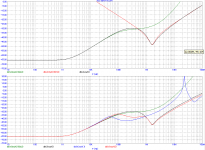
Now, for you aos, I've run a sim using the ADM7150 model I eyeballed from the impedance curve.
First graph, top :
Red : Z of 10u MLCC
Green : Z of regulator alone
Black : Z combined (pretty much identical to the simulation posted by the ADI guys)
Bottom :
Black : Zout with 10u MLCC
Blue : 220u Polymer + 10nF (using realistic ESL)
Red : 47u polumer + 10u MLCC
You can see it matches your circuit behaviour : 10nF creates huge peak, 10u alone is perfect, 47u polymer is mostly useless but doesn't hurt that much
Second plot is transient response, same colors, you can see the 10nF cap turns the simulated reg into a nice oscillator, and the big polymer makes the transient peak smaller, but much longer, with a little bit of wobbling at the tail, which doesn't look so good.
So this reg is simple to use because it has a smart compensation, but how it works out depends on the output caps. The ADI guys know their stuff, if they optimized it for 10u MLCC, and they recommend a 10u MLCC, just stick a 10u MLCC and don't lose sleep over it.
If you want a reg that is stable with almost anything that has enough capacitance, then it will have 0.2 ohms Z at DC, like ADP151 or TL431. Note that it will still fail with 10 or 100nF capacitor...
> Can those "two peak" graphs be drawn using a function generator (say sweep from 100kHz to 10MHz) and an oscilloscope?
Yes you can do that. I use a network analyzer. Simulator works also.
But the ultimate test is transient load test, just use a 74AC14 to make a square wave, send it to regulator output with a suitable resistor, and look at voltage on scope. If you get same response as ADM7150 datasheet without over/undershoot, ringing, etc, then you did a good job.
Attachments

Last edited:
Wow, that is amazing amount of info, thank you. Can you tell me how do you simulate a regulator with given poles and zeroes? Using (demo) microsim or ltspice, is there a way to specify response like that? Obviously you can create a full transfer function as a ratio of two polynomials if you know where poles and zeroes are - is there a way to specify a "black box" with such transfer function to serve as regulator?
You can use a laplace transform dependent source and enter your expression, works fine in AC analysis on my simulator but not so much in transient.
So I use the idiot mode : dependent sources (current/voltage) and RC between them to make the poles... works fine in transient and AC...
So I use the idiot mode : dependent sources (current/voltage) and RC between them to make the poles... works fine in transient and AC...
Attachments

Thanks very much for your help, my DAC is now working well and I have a lot to think about and experiment.
Btw I never thought of Panasonic SMD polymers as fashionable, I've been using them for a decade and I've never seen anyone else using them. But I do live under a rock these days.
Btw I never thought of Panasonic SMD polymers as fashionable, I've been using them for a decade and I've never seen anyone else using them. But I do live under a rock these days.
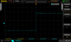
Here are a few measurements just to accompany the theoretical ones. Output of 5V ADP7150 was fed 1.5V square wave at 1kHz through a 100Ohm resistor. When a smd polymer is added, we can see peaking and the oscillation is not well damped. The normal (2 x 10uF ceramic) response is slower but no peaking and no long term oscillation. Keep in mind the function generator while capable of up to 40MHz square and 100MHz sine doesn't have the sharpest rise to begin with and I'm not happy with probe connection (I did solder a spiral piece of wire to get the shortest possible probe ground right across the ceramic but it was too thin and seemingly intermittent). Interestingly enough when a 120uF low esr cap (not polymer) is added, the response seems to be best to my eyes. Still in all these cases the effect seems fairly subtle on oscilloscope.
Attachments
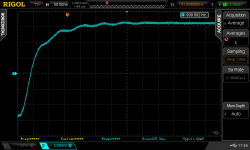
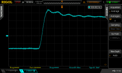


Best way to observe those is to solder coax directly to board. Solder coax GND braid to GND plane, add 50R (or 47R) in series with coax center conductor, use 1X setting on scope.
Your ripple at about 13 Mhz (75 ns period) looks funny, I wonder where it comes from...
Your ripple at about 13 Mhz (75 ns period) looks funny, I wonder where it comes from...
Best way to observe those is to solder coax directly to board. Solder coax GND braid to GND plane, add 50R (or 47R) in series with coax center conductor, use 1X setting on scope.
...
Good point. The late Jim Williams published a tutorial on "good probing" in 1991 -- Application Note 47 on Linear Tech's website:
http://cds.linear.com/docs/en/application-note/an47fa.pdf
- Status
- Not open for further replies.
- Home
- Amplifiers
- Power Supplies
- Modern ultra low noise LDO - ADM7150