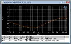
I wouldn't recommend floating the ground of the ADM7150 as this could lead to permanent damage to the device if the output is ever shorted.As I just mentioned on another thread for low noise regulators, you're wasting your time using anything but the ADM7150 if noise is the spec you have to optimize. I just ran the device with a 50mA load and a 5uF bypass capacitor and come up with exactly the values shown on the datasheet.
I used the SOIC-8, and attached the device to an SOIC adapter using copper tape as the thermal pad.
The ADM7150 can be used as an adjustable regulator -- see the data sheet for the evaluation kit. I would imagine that you could use it for higher voltages by lifting the ground pin with a zener (not avalanche) diode, or using a pass transistor/mosfet such that the Vin/Vout limit isn't broached.
The ADM7150 is essentially two LDOs is series. The first LDO is rated for ~16V max whereas the second (low noise) LDO is only rated for 5.5V. If the output voltage is greater thant 6V and the output is shorted to ground, the maximum voltage of the low noise LDO stage will be violated. This can lead to the failure of the pass transistor due to excessive voltage stress.
So if you float the ground pin, inrush and shorts could kill your chip because the output would be shorted for a moment, causing excessive input voltage. These situations can be avoided given some effort, so for careful designs by knowledgeable people it should be okay.
So if you float the ground pin, inrush and shorts could kill your chip because the output would be shorted for a moment, causing excessive input voltage. These situations can be avoided given some effort, so for careful designs by knowledgeable people it should be okay.
A 5.1V Zener, anode to output, cathode to input, MJD44H11 pass transistor etc. etc.
The GND pin pumps out several MA ....
Floating ADM7150
I'd probably go with a 600mA/5.1V zener from Vreg to Vout on the ADM7150. Vreg is internally set to ~600mV above Vout. This way, if the output ever gets shorted to ground the low noise LDO pass transistor should be protected.
The ground current is a function of the load current so you'll want to be able to sink at least 15mA. The current sink must also be very low noise or it will also add to the total output noise.
A 5.1V Zener, anode to output, cathode to input, MJD44H11 pass transistor etc. etc.
The GND pin pumps out several MA ....
I'd probably go with a 600mA/5.1V zener from Vreg to Vout on the ADM7150. Vreg is internally set to ~600mV above Vout. This way, if the output ever gets shorted to ground the low noise LDO pass transistor should be protected.
The ground current is a function of the load current so you'll want to be able to sink at least 15mA. The current sink must also be very low noise or it will also add to the total output noise.
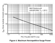
But then your zener has to be able to handle the inrush. Does anyone know the max surge current for a given zener?
If you know the short circuit output of your trafo you can make sure capacitances are chosen to keep zener current at least within it's DC ratings.
If you know the short circuit output of your trafo you can make sure capacitances are chosen to keep zener current at least within it's DC ratings.
Have a look at the manufacturer's datasheet, some include a max surge power curve. I try to design for less than 0.01% duty cycle when operating anywhere near the max limit, to let everything cool off and relax after taking such an enormous body-blow. It's merely my opinion of a reasonable way to extend the life of the diode; others have different opinions.Does anyone know the max surge current for a given zener?
Here's the MMS18ZE from ON Semiconductor.
Attachments
Last edited:

Jack, I looked at the datasheet for "MRA" noninductive wirewound resistors from Vishay Mills, and didn't see an inductance specification.... for comparison/reality checked I included a Mills 100mΩ ...
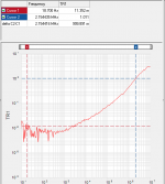
Your plot seems to show that the 0.1 ohm resistor becomes inductive at ~ 22 kHz, which corresponds to an inductance of 700 nanohenrys. Do you think that's the actual inductance of the resistor, or an artifact of the test fixture & software?
About 0.5μH
In the LF region which I was addressing, I get the same result using the Bode100 Analyzer so the simulation would appear to be off by an order of magnitude.
In the LF region which I was addressing, I get the same result using the Bode100 Analyzer so the simulation would appear to be off by an order of magnitude.
Which DC load on the reg ? More current should give more Gm and lower Zout...
Most LDOs perform rather poorly at low load currents, because the PMOS lacks Gm...
Also, unless it is your intention to power down the load, the load current should never drop to zero. When that happens, the LDO will block its PMOS, but that takes a while, and during that time some current is still flowing, which goes in the output caps and causes overshoot, especially if they're small, like a few uF ceramics. Then the LDO will wait until the output voltage drops again, and re-bias the PMOS to let some current flow. But that, too, takes a while (most regs are pretty slow).
If the load goes from zero current to, say, a few mA, by the time the LDO reacts, the output capacitor already has discharged a bit, so the LDO will send a lot of current in the output to bring the voltage back to normal.
This is how a load switching between 0 and 1mA, with the right frequency and capacitors, will make the LDO pull fast 50-100mA (or more) spikes from the power supply, happily passing the noise to the neighbors sharing the same supply.
You can check that out with your impedance measurement setup, by playing with the DC load and setting it so the sum of DC load + AC current injected by the impedance probe juuuuust touches zero, and looking at the waveform on a scope. The input current waveform tends to get massively ugly. Some LDOs are a lot less ugly than others.
It is clipping, just like an amplifier, some do it clean, some just lose it.
Interesting post peufeu!
I wonder what you are describing is not some oscillation tendency because the reg moves into an area with low load where the gain is too high to reman stable, with that particular output cap? You'd want a good reg to be stable also at this regimen.
Jan
I wonder what you are describing is not some oscillation tendency because the reg moves into an area with low load where the gain is too high to reman stable, with that particular output cap? You'd want a good reg to be stable also at this regimen.
Jan
It isn't oscillation, just plain clipping and slew rate limiting... In an opamp, "clipping" refers to output voltage hitting the wall, at which point some stuff happens (transistors may get blocked or saturated, compensation caps get overcharged, etc) which may take time to recover ; slew rate limit is clipping of the input stage (more precisely in a standard topology it is hitting the maximum current which the circuit can push in the Cdom capacitor), in this case also it needs time to recover, for instance if the input pair saturates.
The important point is that when clipping happens in any part of the circuit, normal closed-loop control does not operate anymore and the circuit is basically banging its head against the wall, waiting for the wall to go away. While this happens, the compensation capacitors, whose job it is to integrate some variable, integrate bogus values instead, and this error accumulates over time (it is integrator windup). When going back to normal, linear operation, closed loop control, all these errors have to be cleaned, saturated or blocked transistors have to go back to linear mode, capacitors have to go back to normal voltages, which takes a while, and not all parts of the circuit come back to life at the same time, which may produce various funny looking glitches. You can see that in the ExtremA thread for example.
For a LDO it is the same : the big fat PMOS is slow and its gate is a big capacitor, the drive circuit can push or pull a limited amount of current into it, so a LDO has a slew rate, but it is a current slew rate : dI/dt instead of dV/dt. It depends on the PMOS Gm, so it gets better at high load.
A LDO can clip also, again same as an opamp with current instead of voltage, when the current in the PMOS reaches zero, the control loop is inoperative. It may saturate the driver, bias the PMOS gate to zero, etc. When it is time to go back to linear operation, the driver will have to desaturate, then drive the gate back from 0V to minus some volts so the PMOS conducts again, that takes a while.
Also, the compensation cap is the output cap, and it integrates the error between load current and LDO output current. And it isn't 33pF like in an amplifier, it's maybe 1 million times larger.
So it isn't oscillation, because once the mess is cleaned up, everything is back to normal. Simply, while the mess is being cleaned up, stuff can happen. Example :
- Output current reaches zero
- LDO puts PMOS to sleep
- Load starts to draw some current, output cap voltage droops
- LDO wakes up, kicks PMOS for about 10-100µs to wake it up, nothing happens, gate driver is clipped
- PMOS reaches threshold, current starts to flow in the PMOS
- At this point the LDO control loop is still not working (it is clipped)
- The PMOS current keeps rising, at some point it exceeds the load current and starts charging the output cap, voltage rises
- At some point, the closed loop control resumes. The PMOS is pushing high current in the output capacitor, so the loop will need some time to bias the PMOS gate to the correct value, there will be some overshoot, normally it is well damped, so there is no oscillation. If the output capacitor is too small, then the overshoot is too large, and the LDO shuts down again, and you get large signal oscillation (not small signal oscillation predicted by bode plot, more like a multivibrator).
That's why an innocent LDO will draw large current pulses from the power supply when coming out of sleep, adding a dummy resistor load isn't such a bad idea to avoid that...
Does a resistive load or a self at the output of the LDO reg can fix the problem without wasting its job and final SQ ? And a huge cap near the load... to have finally a stable and continous feeding of this final decoupling and power cap, this last one feeding the load with the best transcient possible (as the cap is huge : i.e. > from the one of the PS before the LDO ? A very low esr cap like a Nichicon KH have big impedance value, very low esr, not polymer: so sound good for analog and also a good inductance for the impedance values involved!)
Sorry for two cents question and my poor understanding, I'm lost in the question of PSRR and transcient ! Also between osclillation & clipping !
Sorry for two cents question and my poor understanding, I'm lost in the question of PSRR and transcient ! Also between osclillation & clipping !
Yes it is actually very simple, if you add a resistor as a dummy load, it will :
- pre-bias the LDO, giving it higher transconductance and lower Z
- ensure current never reaches zero
But if your load is a few opamps which always draw some idle current, no need to worry. It is mostly if the circuit being powered can sleep and draw very low currents, then wake up periodically, like a microcontroller, that you can get this effect.
Jack, you're getting something like 5 mOhm at low freq in your last graph, I don't see reason to complain about that...
Last edited:
Jack, you're getting something like 5 mOhm at low freq in your last graph, I don't see reason to complain about that...
If the opamp's open loop DC gain is 110 dB, and if the feedback network's voltage division ratio is 1/3rd (gain of -10dB), and if the pass transistor's gain is 0.9X (-1 dB) then the total loop gain is 99dB or so.
If the regulator's open loop output impedance is ~ 1 ohm (opamp open loop output impedance divided by pass transistor beta, plus emitter follower output impedance (1/gm)), then we expect the closed loop output impedance to be 99dB below 1 ohm. Namely, eleven micro-ohms.
The surprise is that Jack's instrumentation jig CAN measure impedances this low, but he ain't seeing what he expects to see.
The surprise is that Jack's instrumentation jig CAN measure impedances this low, but he ain't seeing what he expects to see.
It's Walt's setup, not mine! He probed the circuits for the lowest impedance output nodes. He was able to measure to 1μΩ.
http://waltjung.org/PDFs/Regs_for_High_Perf_Audio_1.pdf
To measure 1μΩ @50mA = 50nV So you need short twisted pair.
5mΩ aint shabby by any means!, and the PSRR and noise readings are just great. I have to configure to take a serious listen with my Borbely all JFET preamp.
Last edited:
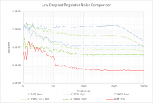
Comparison with LT1084, LT1963A -- the LT1084 is also shown with the adjust leg bypassed with 10uF, the LT1963A with Cff of 1uF+1K and 10uF, the ADM7150 per the application notes.
Of course, the ADM7150 isn't gained up like the two LTC regulators so the noise of its error amplifier and reference is going to be lower -- it's output is 5V, vs 13.4V.
Of course, the ADM7150 isn't gained up like the two LTC regulators so the noise of its error amplifier and reference is going to be lower -- it's output is 5V, vs 13.4V.
Attachments
- Status
- Not open for further replies.
- Home
- Amplifiers
- Power Supplies
- Modern ultra low noise LDO - ADM7150