Also when probing a digital circuit the probes loading will affect the waveform, especially with todays faster rise time etc. When I do simulations I also have models of the probes that are going to be used so the engineer gets the same image from simulation as he does from the scope screen. Most probe manufacturers provide the required data for modelling a probe...
Best way to observe those is to solder coax directly to board. Solder coax GND braid to GND plane, add 50R (or 47R) in series with coax center conductor, use 1X setting on scope.
Your ripple at about 13 Mhz (75 ns period) looks funny, I wonder where it comes from...
The method I used was another classic recommended method, a few turns of bare wire around the probe body (ground sleeve) and soldered to the ground right next to probing point. Coax would work because of low impedance in our case but this approach is more generic. I just chose a wire that wasn't stiff.
The "13Mhz" might be modulation from the digital bit clock which is 12.28 Mhz (and master clock is 2x that) which is fed into the DAC chip which is the only thing powered by the regulator. Some of those screenshots are 20MHz BW limited, some are not in which case I get another superimposed higher frequency ripple (could be the master clock). Or it could be function gen or some environment noise.
Nice thread guys.
So if we want to use ADM1750 with a dac, we should not use the proposed decoupling 100nF caps on the dac's power pins?
Any suggestions on eliminating that noise, or should the ADM7150 be able to handle it? Some dacs really needs those caps. I was thinking really short interconnecting lines but would it be enough? Oh and really this means forget about daughterboard regs or TO220 replacement thingies.
I am thinking to use it with 33uF ceramics (as gmorita verified it was tested ok with such values) to give it some more transient muscle.
Oh and I really have to ask... would there be any issues wiring them in series for dual rails?
Last edited:
So if we want to use ADM1750 with a dac, we should not use the proposed decoupling 100nF caps on the dac's power pins?
You better keep decoupling caps close at the pins of the DAC chip but I guess loading the reg with 100 nF will not work optimal. I never encountered a DAC chip that could do without decoupling the pins. You could use 10 µF directly at the pins if the reg feels better with those.
Cascading the ADM7150 is not an issue as along as the input voltage to the second ADM7150 is greater than 4.5V and to total load current is less than 800 mA.Nice thread guys.
So if we want to use ADM1750 with a dac, we should not use the proposed decoupling 100nF caps on the dac's power pins?
Any suggestions on eliminating that noise, or should the ADM7150 be able to handle it? Some dacs really needs those caps. I was thinking really short interconnecting lines but would it be enough? Oh and really this means forget about daughterboard regs or TO220 replacement thingies.
I am thinking to use it with 33uF ceramics (as gmorita verified it was tested ok with such values) to give it some more transient muscle.
Oh and I really have to ask... would there be any issues wiring them in series for dual rails?
Some dacs really needs those caps. I was thinking really short interconnecting lines but would it be enough?
Actually when you put a decoupling cap in your design, it is not about the capacitance, it is about the inductance, ie, giving a low inductance power supply to the chip.
Note I'm not talking about powering a fat ASIC or FPGA with 20 or 50 power/GND pin pairs and power planes etc. Just a DAC, which is going to have something like maybe 1 AVCC and 1 AGND pin, or two. In this case :
- The inductance of the pins, bondwires, etc, all that adds up to a few nH. You can't get below that unless you put the decoupling caps inside the chip or you have 50 power/GND pins. So if you put 1 MLCC right on the avcc/agnd pins, that's pretty much optimal. Yes you can put more caps... that won't reduce the pin inductance though, so it probably isn't going to matter.
- So... just use the largest cap you can get in a small package, for example a 10uF X7R in 0805, and stick it right at the power pins. If the chip has a user-friendly layout (ie, avcc/agnd pins next to each other) that's nice.
Your 10uF 0805 has exactly the same inductance as a 100nF cap in same package size, so it is just "as fast" (as far as there is such a thing as fast or slow cap...)
And you put your LDO very close, and do the layout so whatever pin the LDO uses as reference (GND, or GND-Sense) goes where it should.
Oh and really this means forget about daughterboard regs or TO220 replacement thingies.
Those don't work because they can't work, unless you add extra pins for GND reference...
Damn high frequency design....
Perhaps the 100nF caps are considered faster because of their higher self resonance allowing lower Q
About layout, I remember reading somewhere that using reverse packages helped a lot. Like 0612. This reduces the L on the cap and allows a bigger connection to the pcb further lowering its inductance (2-3 ground plain vias perhaps too?) They even suggested the possibility of adding more caps piggyback. Like 100nF on the bottom and 10uF on top.
Would that make sense?
Actually if you take a MLCC like 0603, 0805, 1206 the difference in ESL isn't that huge, they're all around something like 0.5-0.6 nH (ok... the smaller ones have a bit less but it's not night and day)... however a via adds more than 1nH, and if there's a bit of trace it adds more loop area, so it's all about the layout & mounting.
Check out example 3 here :
LearnEMC: Estimating the Inductance of a PCB Connection
If you're going to hand solder the board (and you don't care about solder wicking down the vias during reflow and turning your caps into little tombstones) the lowest ESL mounting for standard caps is this :
Check out example 3 here :
LearnEMC: Estimating the Inductance of a PCB Connection
If you're going to hand solder the board (and you don't care about solder wicking down the vias during reflow and turning your caps into little tombstones) the lowest ESL mounting for standard caps is this :
Attachments
Nice article
Basically example 3 shows exactly what I proposed. The reversed packages 0612 should have even less inductance.
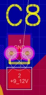
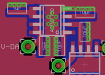
Here is what I have as a first draft.

What I am worrying about is that it is going to be HARD to hand solder those vias without thermals (which would negate the whole point if added to the vias)
Basically example 3 shows exactly what I proposed. The reversed packages 0612 should have even less inductance.
Here is what I have as a first draft.
What I am worrying about is that it is going to be HARD to hand solder those vias without thermals (which would negate the whole point if added to the vias)
Attachments
The trace inductance will probably be much higher than the inductance of the 0612 caps, so you can use them if you like, but don't lose sleep over it...
I would just use 2 10uF ceramics, one right at the regulator as required and the other right at the DAC. That is what I eventually settled on, though the experiments show a normal (non ultra low) esr electrolytic might help as well to keep the transient response nicer. I am thinking of buying an active probe to help me see what's going on.
Since we are told the regulator was tested with up to 30uF ceramics (3x10 on the demo board?), keeping one at the regulator and the other (or two) at the DAC seems reasonable. If you put that 100nF instead, you will get instability just like I did.
Since we are told the regulator was tested with up to 30uF ceramics (3x10 on the demo board?), keeping one at the regulator and the other (or two) at the DAC seems reasonable. If you put that 100nF instead, you will get instability just like I did.
- Status
- Not open for further replies.
- Home
- Amplifiers
- Power Supplies
- Modern ultra low noise LDO - ADM7150