I have known of an issue just like this and in my case it is not produced at the board house. The issue is in a mismatch between what you see on the screen in Eagle edit mode and the creation of the Gerber files (the master images used to manufacture the boards). You should create the Gerber files yourself, then view them carefully with a suitable viewer before you submit them to the board house. The Gerber files will be faithfully reproduced. If you leave the board house to create your Gerber files you can get all sorts of issues. The default in Eagle is to use variable width fonts and these often don't convert well when making Gerbers - at least that is what I have found. So I used fixed width (they are a bit boring!) fonts and then I check the Gerbers - in many cases I still have to adjust the position of text as there is sometimes an offset between what you see in Eagle edit and what shows up on the Gerbers. Check and double check your Gerber files and you'll be fine.
Hi Gareth, actually, my PCBs (post #155 above) are also produced in a board house, based on exactly the same P-CAD ASCII file, and the silk screen looks fine. So the font was changed somehow in Terry's board house, though in P-CAD viewer it looks the same and looks fine. Weird...
Hi Valery,
I notice in the pics you show of the pics you show in post #107, that you have some pretty large resistors in R6 & R9. Do these need to be high wattage?
Do you have an .asc file for this? That would be helpful.
My small transformer should be here today. I will be able to do some testing. Is there a special sequence for start up? Should the 6.3V transformer be turned on first? If so, for how long before the other? I will be using a variac and light bulb for initial testing but not sure how a tube reacts to varying voltage.
Thanks, Terry
Hi Valery,
I notice in the pics you show of the pics you show in post #107, that you have some pretty large resistors in R6 & R9. Do these need to be high wattage?
Do you have an .asc file for this? That would be helpful.
My small transformer should be here today. I will be able to do some testing. Is there a special sequence for start up? Should the 6.3V transformer be turned on first? If so, for how long before the other? I will be using a variac and light bulb for initial testing but not sure how a tube reacts to varying voltage.
Thanks, Terry
Hi Terry,
R6 and R9 are actually 22K each and they don't have to be high wattage - 0.25W will do fine there.
Start-up sequence (at least for initial testing) - switch the small "heating" transformer on first, wait 20 seconds, switch on all the rest.
Later on, if everything is fine, you can try switching on all the rest right away - output will fluctuate up to the rails, but the main point - it stays stable (no oscillation), so no problem.
Wishing you a pleasant power-on 😉
Cheers,
Valery
Thanks,
Was it determined if any of the transistors should be thermally coupled?
Not mandatory, but in principal will improve thermal stability, if three pairs are coupled:
Q6-Q10
Q11-Q16
Q13-Q14
Cheers,
Valery
Ok, my transformer came in, so with great expectations I began testing. I first hooked up each individual IPS using 470R resistors as load resistors fed to the NFB. The first board I tested finally settled at about 80mv offset. It doesn't settle completely but wanders up and down +-10mv. I get about 4.9V across the two 470R resistors so about 5.2mA output. I then bypassed the 470R load resistors and the offset remained the same. I set that board aside and tested the other. It settled at about 5mv offset but still varied +-10mv. Then I hooked up the first one again and swapped the tubes and it then settled at about 25mv offset. Things looked pretty good so I hooked them up to the OPS. I brought it up on the variac and light bulb tester and before I could get it half way up the negative side LED began to flash on an off and the light bulb tester shown bright. So then I backed the bias on the OPS all the way down and tried again. I was able to get the right channel to come up to full rails but not the left so I unplugged that side and tried working with just the right channel. With the light bulb tester in place I could get it up to full rail but it would surge about ever 6 seconds. The light would go bright and the bias would shoot up on the outputs. I thought maybe the light bulb was causing the surging so I bypassed the light bulb and went direct. I was still seeing the bias shoot up about every 6 seconds or so and then it blew the fuses. I guess I need some ideas on what to look for. I'm going to go back to just the IPS and try passing a sine wave through it. I'll report back.
Thanks, Terry
Edit; I forgot to mention that if I shorted PD+ to ND_ with the OPS hooked up, the LEDs stopped flashing.
Thanks, Terry
Edit; I forgot to mention that if I shorted PD+ to ND_ with the OPS hooked up, the LEDs stopped flashing.
Last edited:
Terry, it looks like as soon as you connect the OPS, you get some oscillation.
So, yes - try to pass a sine, with just the IPS, then, when you connect the OPS - monitor the output with the oscilloscope.
Cheers,
Valery
So, yes - try to pass a sine, with just the IPS, then, when you connect the OPS - monitor the output with the oscilloscope.
Cheers,
Valery
Terry, it looks like as soon as you connect the OPS, you get some oscillation.
So, yes - try to pass a sine, with just the IPS, then, when you connect the OPS - monitor the output with the oscilloscope.
Cheers,
Valery
Hi Valery,
I just got back from testing the IPS alone. It plays sine and square waves beautifully. I can't test the output of the OPS with this IPS attached because it surges too badly. Something is just not happy. There is nothing wrong with the OPS. I disconnected the Wolverine IPS to hook this one up.
Am I right in assuming that that PD+ is on the same side as V+ and ND- is on the same side as V-?
Thanks, Terry
I'm wondering if this IPS has too high of an output. Almost all of the other IPS I've built are outputting about 4.2mA. This one is 5.2mA. How do I lower the output? I'd like to try that before I start replacing caps al over the place/
Thanks, Terry
Thanks, Terry
I'm wondering if this IPS has too high of an output. Almost all of the other IPS I've built are outputting about 4.2mA. This one is 5.2mA. How do I lower the output? I'd like to try that before I start replacing caps al over the place/
Thanks, Terry
Hi Terry, sorry for delay - today is a training day, just back to earth from the sky 🙂
Yes, lowering the output current may help. You can do it increasing R17 from 180 ohm to 220-270. Try it without the OPS first.
Hi Valery,
I know it's late there so you probably won't get this till morning. I tried changing R17 to 220 and no change to the problem. The IPS is fine alone. Once it is hooked up to the OPS it starts surging badly. I sat down and measured each resistor and transistor for vR and vRE and jotted them down. This is without the OPS hooked up. The input is shorted and PD, ND and NFB are shorted together. When you get a chance, Please take a look and see if everything looks about right. As I said, the IPS works fine alone. The OSP works fine attached to my other IPS units.
Shame you don't have a Slewmaster OPS built that you can test this with.
Blessings, Terry
Attachments
Hi Valery,
I know it's late there so you probably won't get this till morning. I tried changing R17 to 220 and no change to the problem. The IPS is fine alone. Once it is hooked up to the OPS it starts surging badly. I sat down and measured each resistor and transistor for vR and vRE and jotted them down. This is without the OPS hooked up. The input is shorted and PD, ND and NFB are shorted together. When you get a chance, Please take a look and see if everything looks about right. As I said, the IPS works fine alone. The OSP works fine attached to my other IPS units.
Shame you don't have a Slewmaster OPS built that you can test this with.
Blessings, Terry
Hi Terry,
Thank you for very good currents/voltages map.
According to measurements, IPS circuit is well balanved, however, your experience with OPS attached shows there is a "hidden" stability issue (high frequency stability margin is enough when IPS works alone, but getting worth when OPS is attached).
I will come back home today in the evening and work on HF stability more thoroughly. Let's put it on hold on your side - I'm sure I will have a solution when you're back from vacation.
Cheers,
Valery
Hi Valery,
Sounds good. I'll keep an eye on the thread with my phone while gone. Hopefully you can find a solution. I ended up having to replace the outputs on one of the output boards. I hoped it just blew the fuses but it took out the outputs. I will happily wait to try again. 😀
Blessings, Terry
Sounds good. I'll keep an eye on the thread with my phone while gone. Hopefully you can find a solution. I ended up having to replace the outputs on one of the output boards. I hoped it just blew the fuses but it took out the outputs. I will happily wait to try again. 😀
Blessings, Terry
Member
Joined 2009
Paid Member
Maybe try putting (more) series resistance in the signal connection between IPS and OPS in case the interaction between them encourages some negative impedances ?
Also check it isn't something crazy like the output signal ending up too close to the input signal wiring.
Also check it isn't something crazy like the output signal ending up too close to the input signal wiring.
Compensation redesigned
Hi Terry and All,
I have finally finished my tests, so now I'm back with the rock stable version of the front end. I have completely reconsidered and redesigned the compensation scheme, taking in account both conditions - normal operation stability and start-up stability (when the tube is not hot enough, so both LTP and GNFB, connected to it, are not working yet).
It is not tested with two different power sections with no indication of instability whatsoever (both are EF3, but the second one has got CCS-loaded drivers in class "A" - part of my earlier design).
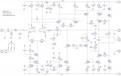
Here is a detailed explanation of the changes:
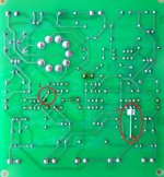
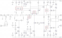
Picture 1 - PCB Bottom
- Cut one trace - marked by the red "X" at the bottom right side of oval "2";
- Solder two new traces - "1" and "2", bearing in mind the "2" one goes over the other trace (I used a small piece of tape to make sure it is insulated properly).
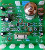
Picture 2 - PCB Top
1) Remove C7. Put 47 ohm resiscor and 220 pF cap serially instead.
2) Remove C13. Put 15 pF instead.
3) Solder 22 pF cap right on top of R16 and R18 pins.
4) Remove C18. Put 22 pF cap instead.
5) Remove C15. Put 22 pF cap instead.
6) Remove C14 and R25 - leave those places blank (marked by red "X"s).
Picture 3 is just an updated schematic for your reference.
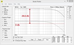
Picture 4 is a new Bode plot after all modifications.
It is still recommended to switch the tube heating on first, and after some 20 seconds power-on everything else.
I tested this one brutally, trying to actually "kill" it. Sound qualities are preserved, while stability is the one I could not break this time.
I really hope it will work for you as well.
Cheers,
Valery
Hi Terry and All,
I have finally finished my tests, so now I'm back with the rock stable version of the front end. I have completely reconsidered and redesigned the compensation scheme, taking in account both conditions - normal operation stability and start-up stability (when the tube is not hot enough, so both LTP and GNFB, connected to it, are not working yet).
It is not tested with two different power sections with no indication of instability whatsoever (both are EF3, but the second one has got CCS-loaded drivers in class "A" - part of my earlier design).
Here is a detailed explanation of the changes:
Picture 1 - PCB Bottom
- Cut one trace - marked by the red "X" at the bottom right side of oval "2";
- Solder two new traces - "1" and "2", bearing in mind the "2" one goes over the other trace (I used a small piece of tape to make sure it is insulated properly).
Picture 2 - PCB Top
1) Remove C7. Put 47 ohm resiscor and 220 pF cap serially instead.
2) Remove C13. Put 15 pF instead.
3) Solder 22 pF cap right on top of R16 and R18 pins.
4) Remove C18. Put 22 pF cap instead.
5) Remove C15. Put 22 pF cap instead.
6) Remove C14 and R25 - leave those places blank (marked by red "X"s).
Picture 3 is just an updated schematic for your reference.
Picture 4 is a new Bode plot after all modifications.
It is still recommended to switch the tube heating on first, and after some 20 seconds power-on everything else.
I tested this one brutally, trying to actually "kill" it. Sound qualities are preserved, while stability is the one I could not break this time.
I really hope it will work for you as well.
Cheers,
Valery
Attachments
Last edited:
any good reason for ruining the PSRR?
caused by the gnd caps "bypassing" the CCS reference - when the CCS are in fact referenced to the negative rail?
caused by the gnd caps "bypassing" the CCS reference - when the CCS are in fact referenced to the negative rail?
any good reason for ruining the PSRR?
caused by the gnd caps "bypassing" the CCS reference - when the CCS are in fact referenced to the negative rail?
Good point in general, however, in this particular case... it does not really matter. There are no PS components visible (or audible) at the output (overall practically measured s/n ratio is more than 110 db)
it gives poor PSRR regardless of whether the PSRR is exercised
negative feedback covers lots of ills - but is no excuse for avoiding best practice when tis only moving a connection of a part you already have on the board
always make a circuit as good as possible open loop when using feedback
negative feedback covers lots of ills - but is no excuse for avoiding best practice when tis only moving a connection of a part you already have on the board
always make a circuit as good as possible open loop when using feedback
it gives poor PSRR regardless of whether the PSRR is exercised
negative feedback covers lots of ills - but is no excuse for avoiding best practice when tis only moving a connection of a part you already have on the board
always make a circuit as good as possible open loop when using feedback
Agree - thank you for pointing this out, will take in consideration for future designs.
Cheers,
Valery
it gives poor PSRR regardless of whether the PSRR is exercised
negative feedback covers lots of ills - but is no excuse for avoiding best practice when tis only moving a connection of a part you already have on the board
always make a circuit as good as possible open loop when using feedback
Is this something that can be addressed now so we don't have to continue to alter the boards? I have some extra boards so it isn't a huge deal but it seems you think it can easily be fixed.
- Status
- Not open for further replies.
- Home
- Amplifiers
- Solid State
- Low TIM, low distortion hybrid front-end