I like class-b amplifiers for their effectiveness. If they are implemented as neatly as by LKA, all the more. Class-d are therefore also on my hit list, but two big advantages of class-b to class-d are: Not necessarily SMD and no hard high frequency.Looks nice and interesting, what's the main advantage of this topology?
The same goes for current dumping.
Personally, I'm currently working on a class b / c amplifier, in which the power transistors are switched on from a certain current. The low quiescent current is only caused by the driver and voltage amplification.


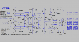
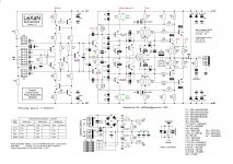
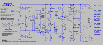
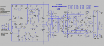
The final LeXaN buffer schematic (voltage amplification =1). I applied Technics synchronous bias technique to the outputs. The cross-over region is very smooth, though the idle bias is 3mA per pair. The circuit doesn't suffer from cross-conduction at high frequencies and output levels (the Achilles heel of almost all Class-B implementation).
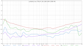
Simulated THD <= 0.01% 0.1W-100W/4R
IMHO, this is the best Class-B output stage I have ever seen.

Simulated THD <= 0.01% 0.1W-100W/4R
IMHO, this is the best Class-B output stage I have ever seen.
Attachments

Last edited:
The final LeXaN buffer schematic (voltage amplification =1). I applied Technics synchronous bias technique to the outputs. The cross-over region is very smooth, though the idle bias is 3mA per pair. The circuit doesn't suffer from cross-conduction at high frequencies and output levels (the Achilles heel of almost all Class-B implementation).
Simulated THD <= 0.01% 0.1W-100W/4R
IMHO, this is the best Class-B output stage I have ever seen.
Very interesting and nice build LKA! What's the loop feedback of the circuit, could you show simulation graph and fft to see the harmonics content?
Last edited:
Did you mean the buffer performance ? What frequencies/levels are you interested in ?
Until now I built and measured LeXaN v1 and v2, just small differences between them.
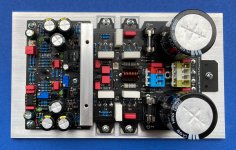
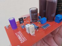
The buffer pcb is in final preparation phase, tomorrow will be send to manufacturing.
Until now I built and measured LeXaN v1 and v2, just small differences between them.
The buffer pcb is in final preparation phase, tomorrow will be send to manufacturing.
Last edited:
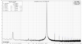
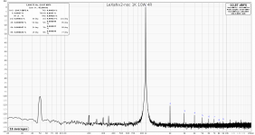
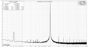
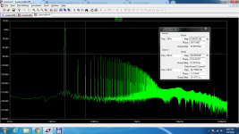
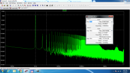
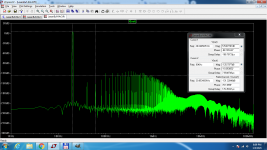
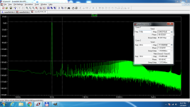
the buffer simulated spectrum at 1W/4R, 1kHz and 20kHz
Attachments
Last edited:
Next step will be a rail switched (class-G) version. I'm planning to use MCU as controlling element. Strange ?
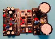
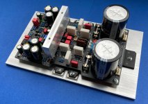
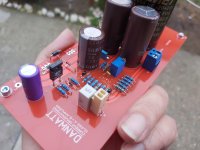
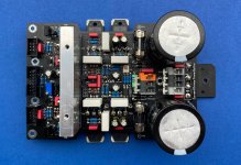
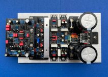
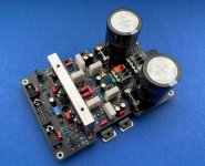
the finished buffer


Attachments
Last edited:
You always surprise me with the parts orientation at least!
Very professional job!
Congratulations.
Very professional job!
Congratulations.
The placement of the components and their color choice are perfect. Absolute alignment on vertical and horizontal axes is also exemplary. You seem to have complete control over the design of printed circuit boards.
- Home
- Amplifiers
- Solid State
- Low distortion current driven Class-B output stage