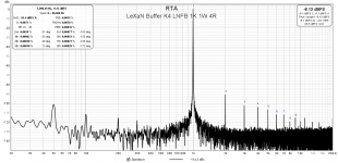
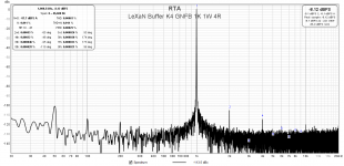
some measurments (global feedback was not applied)
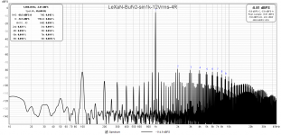
spectrum 1W/4R 1kHz and 10kHz


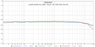
THDvF 1W 10W 50W /4R

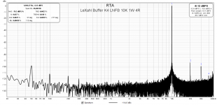
spectrum 1W/4R 1kHz and 10kHz
THDvF 1W 10W 50W /4R
Attachments
When global feedback is applied, even harmonics are less reduced than odd ones. What could be the explanation?
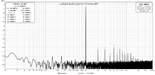
1W/4R 1kHz, no global feedback
2H 0.0028% -91dB
3H 0.00077% -102dB
4H 0.00062% -104dB
5H 0.00051% -106dB
1W/4R 1kHz, global feedback
2H 0.00053% -106dB
3H 0.000026% -132dB
4H 0.00022% -113dB
5H 0.000030% -131dB
Distortion reduction by global feedback
H2 15dB
H3 30dB
H4 9dB
H5 25dB

1W/4R 1kHz, no global feedback
2H 0.0028% -91dB
3H 0.00077% -102dB
4H 0.00062% -104dB
5H 0.00051% -106dB
1W/4R 1kHz, global feedback
2H 0.00053% -106dB
3H 0.000026% -132dB
4H 0.00022% -113dB
5H 0.000030% -131dB
Distortion reduction by global feedback
H2 15dB
H3 30dB
H4 9dB
H5 25dB
Attachments
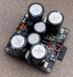
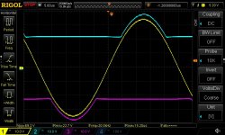
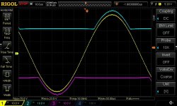
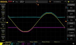
First measurments of the Class B+G prototype.
Outer PSU +-48V
Inner PSU +-24V
Yellow trace = output into 4R
Blue trace = upper/inner transistor collector voltage
Magenta trace = lower/inner transistor collector voltage
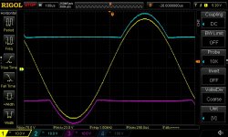
Outer PSU +-48V
Inner PSU +-24V
Yellow trace = output into 4R
Blue trace = upper/inner transistor collector voltage
Magenta trace = lower/inner transistor collector voltage
Attachments
-
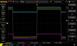 LeXaN-BUFv2-sqr10k-60Vpp-4R.jpg118 KB · Views: 177
 -
 LeXaN-BUFv2-sin20k-70Vpp-4R.jpg129.8 KB · Views: 152
 -
 LeXaN-BUFv2-sin10k-70Vpp-4R.jpg126.6 KB · Views: 220
 -
 LeXaN-BUFv2-sin1k-lim-4R.jpg122.9 KB · Views: 165
 -
 LeXaN-BUFv2-sin1k-70Vpp-4R.jpg129.5 KB · Views: 204
 -
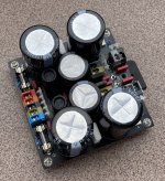
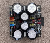
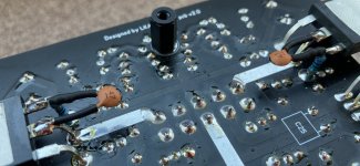
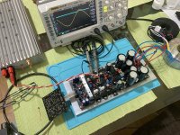 LeXaN-BUFv2-on-bench.jpg712.4 KB · Views: 198
Congratulations!
Looks promising!
You have used IRFPs 240/9140 for higher rail voltages?
what gate resistor values are you using here in your test sample?
Looks promising!
You have used IRFPs 240/9140 for higher rail voltages?
what gate resistor values are you using here in your test sample?
thx
First I tried IRFP240/9140. 9140 was stable with 120R gate stopper, 240 only with 220R. Now I have IRFP140/9140 and 150R stoppers.
First I tried IRFP240/9140. 9140 was stable with 120R gate stopper, 240 only with 220R. Now I have IRFP140/9140 and 150R stoppers.
The distortion is bad when high voltage rails are involved. The transition is somewhere between 11-12 Vrms. The 100Hz modulation is also very strong above the transition line, but acceptable at higher outputs like 18Vrms. Tony, what do you think ? Where is the problem ?
Attachments

r60 and r61: the original design uses 20mA idle current.
have you used the same fast schottky types as our test sample?
have you used the same fast schottky types as our test sample?
"have you used the same fast schottky types as our test sample?"
no, I have used MBR20100CT
what about this one ?
https://www.tme.eu/Document/10a0166a026625918c85178c0a76cca8/DSA20C100PN.pdf
no, I have used MBR20100CT
what about this one ?
https://www.tme.eu/Document/10a0166a026625918c85178c0a76cca8/DSA20C100PN.pdf
Last edited:
During the transition the 100 Hz ripple from the low voltage power supply trigger the schottkys on/off. maybe the LV PS elko ground routing is too near the feedback line.
I solved the problem by increasing the gate stoppers from 150R to 200R. The oscillation was not visible on the oscilloscope. Now the distortion is also excellent above the transition line.
🙂
Congratulations! The IRFPs do not like longer legs!
Have you tried to short circuit the 0.1R resistors R37 and R38 (schematic post #63).
I have used 150R gate resistors as close to gate as possible. (see picture in post #1408).
AFAICS you are using only one MOSFET per rail so current sharing is not a problem. Should better the THD a little bit.
BR, Toni
Last edited:

- Home
- Amplifiers
- Solid State
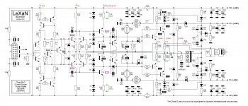
- Low distortion current driven Class-B output stage